

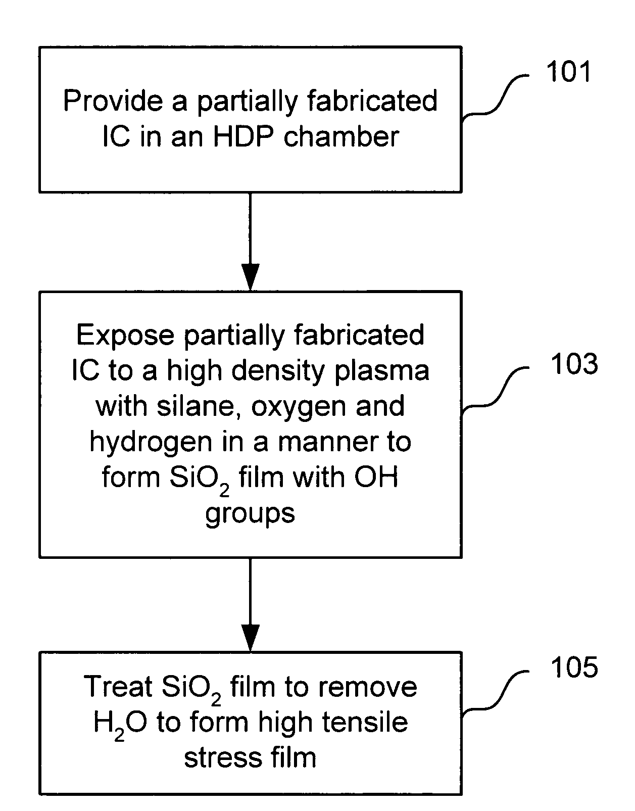
Strain engineering-HDP thin film with tensile stress for FEOL and other applications
a technology of tensile stress and strain engineering, which is applied in the direction of plasma technique, chemical vapor deposition coating, coating, etc., can solve the problems of reducing the effective mass of electrons, consuming too much thermal budget for advanced transistor architectures, and affecting the efficiency of transistor fabrication processes, so as to achieve the effect of not adversely affecting the efficiency of transistor fabrication process
- Summary
- Abstract
- Description
- Claims
- Application Information
AI Technical Summary
Benefits of technology
Problems solved by technology
Method used
Image

Examples
examples
[0047]The following examples are presented to help illustrate aspects of the invention. These examples are representative only, and that the invention is not limited by the detail set forth in these examples. In additions, the following examples show process conditions for depositing and treating high tensile silicon oxide films for experimental purposes and may not necessarily represent optimized conditions for depositing films for any particular specific device application.
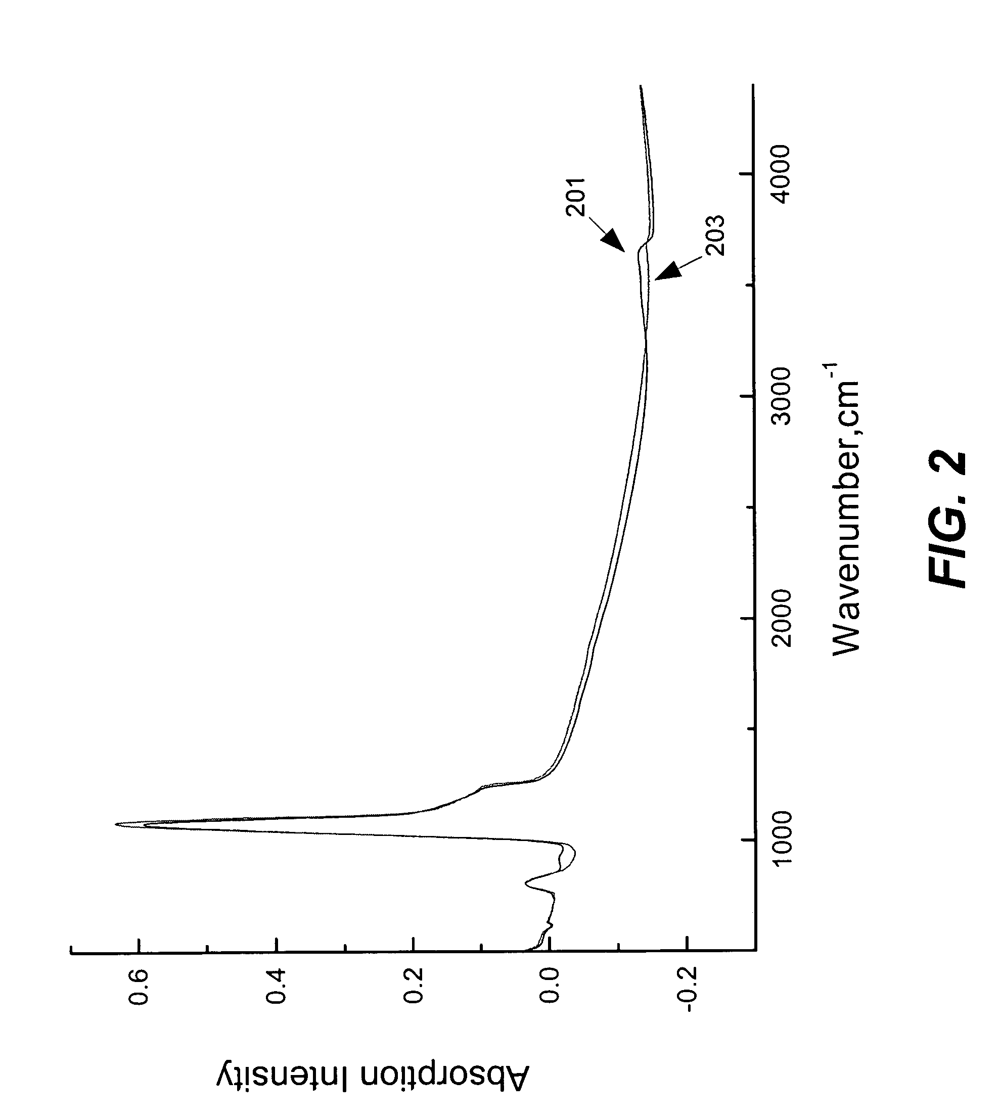
[0048]FIG. 2 is a composite graph showing two FTIR absorption spectra of silicon oxide films formed using methods of the invention. Spectral line 201 is a silicon oxide film after the first phase, HDP deposition. Spectral line 203 is the same film (line 201 film) after the second phase, post-deposition water removal, using a HDP treatment. The process conditions for the deposition process was: 40 sccm SiH4, 1800 sccm H2, 160 sccm O2, 4,500 Watts LFRF, 500 Watts HFRF, ˜300 C substrate temperature, 3.75 cm pedesta...
PUM
| Property | Measurement | Unit |
|---|---|---|
| Temperature | aaaaa | aaaaa |
| Temperature | aaaaa | aaaaa |
| Temperature | aaaaa | aaaaa |
Abstract
Description
Claims
Application Information