Probe manufacturing method, probe, and scanning probe microscope

a manufacturing method and scanning probe technology, applied in the field of probe manufacturing methods, probes, scanning probe microscopes, can solve the problems of insufficient strength of produced probes, inability to achieve sufficient strengthening, insufficient bonding strength, etc., to improve conductivity, increase bonding strength, and improve strength

Inactive Publication Date: 2008-06-17
VIVENTIA BIOTECH +1
View PDF18 Cites 5 Cited by
  • Summary
  • Abstract
  • Description
  • Claims
  • Application Information

AI Technical Summary

Benefits of technology

[0028]According to the method of producing a probe of the present invention, there is provided a method of producing a probe by attaching a nanotube to a mounting base end under observation by an SEM etc. and bonding the them by a coating film etc. wherein a carbon contamination film formed due to the SEM etc. is stripped off at a stage before the bonding work to enable bonding without the effects of the carbon contamination film etc., so the nanotube and mounting base end may be directly bonded, the strength may be improved, and the conductivity may be improved. According to the present invention, when detaching the holder from the nanotube after the mounting work, the contamination film is broken and the surface of the nanotube is exposed.
[0029]According to the probe of the present invention, it is possible to increase the bonding strength and increase the conductivity. Further, by using this probe as an AFM probe, it is possible to utilize this as AFM lithography based on its high conductivity.
[0030]According to the scanning probe microscope of the present invention, by providing a probe having a high bonding strength and conductivity, it is possible to raise the durability of the device and possible to release the charge due to the high conductivity so eliminate the effects of static electricity and thereby improve the measurement accuracy.BEST MODE FOR WORKING THE INVENTION
[0031]Below, preferred embodiments of the present invention will be explained based on the attached drawings.
[0032]Referring to FIG. 1, the method of producing a probe according to a first embodiment of the present invention will be explained. In FIG. 1, 11 indicates a holder (metal sheet), 12 a carbon nanotube, and 13 a mounting base end. The carbon nanotube 12 is produced by for example the electrophoresis method and is obtained in the state attached to the holder 11. The carbon nanotube 12 is a cylindrical member with a cross-sectional diameter of 1 nm to several tens of nm. The mounting base end 13 is for example a probe tip formed at a cantilever used for an atomic force microscope. This probe tip, that is, the mounting base end 13, is usually produced utilizing semiconductor film forming technology etc. The carbon nanotube 12 is attached and bonded to the front end of the mounting base end 13, whereby a probe is assembled and produced.
[0033]In FIG. 1, three partial views (A), (B), and (C) are used to show steps 1 to 3 of the method of production. At step 1, the holder 11 is used to attach a carbon nanotube 12 to the front end of the mounting base end 13. A carbon film is formed (carbon contamination film 14) and a bonding coating film 15 is used to bond the carbon nanotube 12 and the mounting base end 13. At step 1, as shown by the arrow 16, force is applied to separate the holder 11 from the carbon nanotube 12. The results are shown in step 2.

Problems solved by technology

According to the method of producing a probe utilizing a nanotube described in the above Patent Document 1, the problem arises that the produced probe is insufficient in strength.
That is, when bonding the carbon nanotube to the mounting base end, the bonding coating film is formed via the carbon contamination film arising due to SEM observation, so the bonding strength becomes insufficient.
Further, when strengthening a probe made using a carbon nanotube, since only one side is coated, sufficient strengthening is not possible.
Further, since the bonding is via a carbon contamination film, the problem also arises that the conductivity is difficult to secure.

Method used


Image

  • Probe manufacturing method, probe, and scanning probe microscope
  • Probe manufacturing method, probe, and scanning probe microscope
  • Probe manufacturing method, probe, and scanning probe microscope

Examples


first embodiment

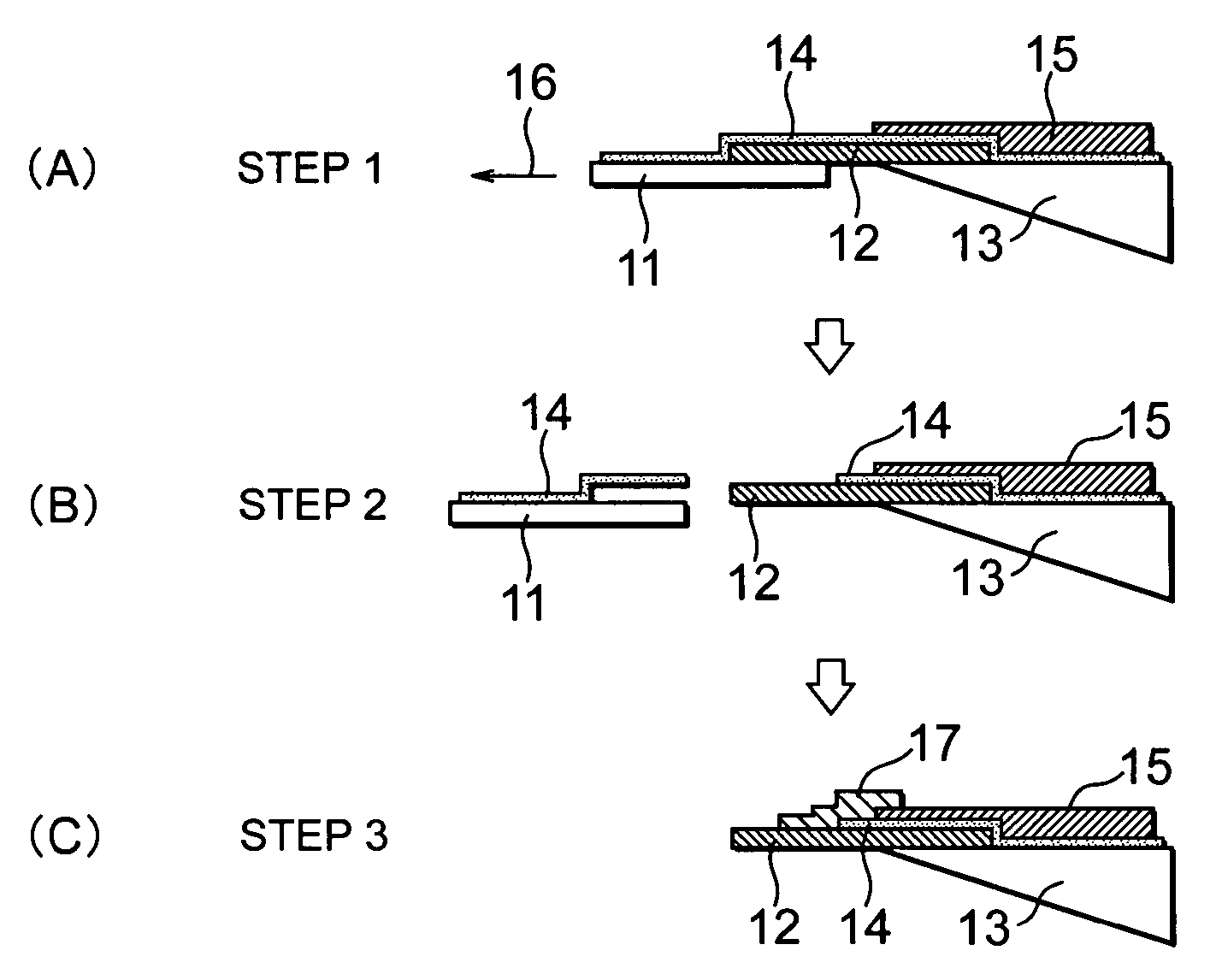
[0032]Referring to FIG. 1, the method of producing a probe according to the present invention will be explained. In FIG. 1, 11 indicates a holder (metal sheet), 12 a carbon nanotube, and 13 a mounting base end. The carbon nanotube 12 is produced by for example the electrophoresis method and is obtained in the state attached to the holder 11. The carbon nanotube 12 is a cylindrical member with a cross-sectional diameter of 1 nm to several tens of nm. The mounting base end 13 is for example a probe tip formed at a cantilever used for an atomic force microscope. This probe tip, that is, the mounting base end 13, is usually produced utilizing semiconductor film forming technology etc. The carbon nanotube 12 is attached and bonded to the front end of the mounting base end 13, whereby a probe is assembled and produced.

[0033]In FIG. 1, three partial views (A), (B), and (C) are used to show steps 1 to 3 of the method of production. At step 1, the holder 11 is used to attach a carbon nanotub...

second embodiment

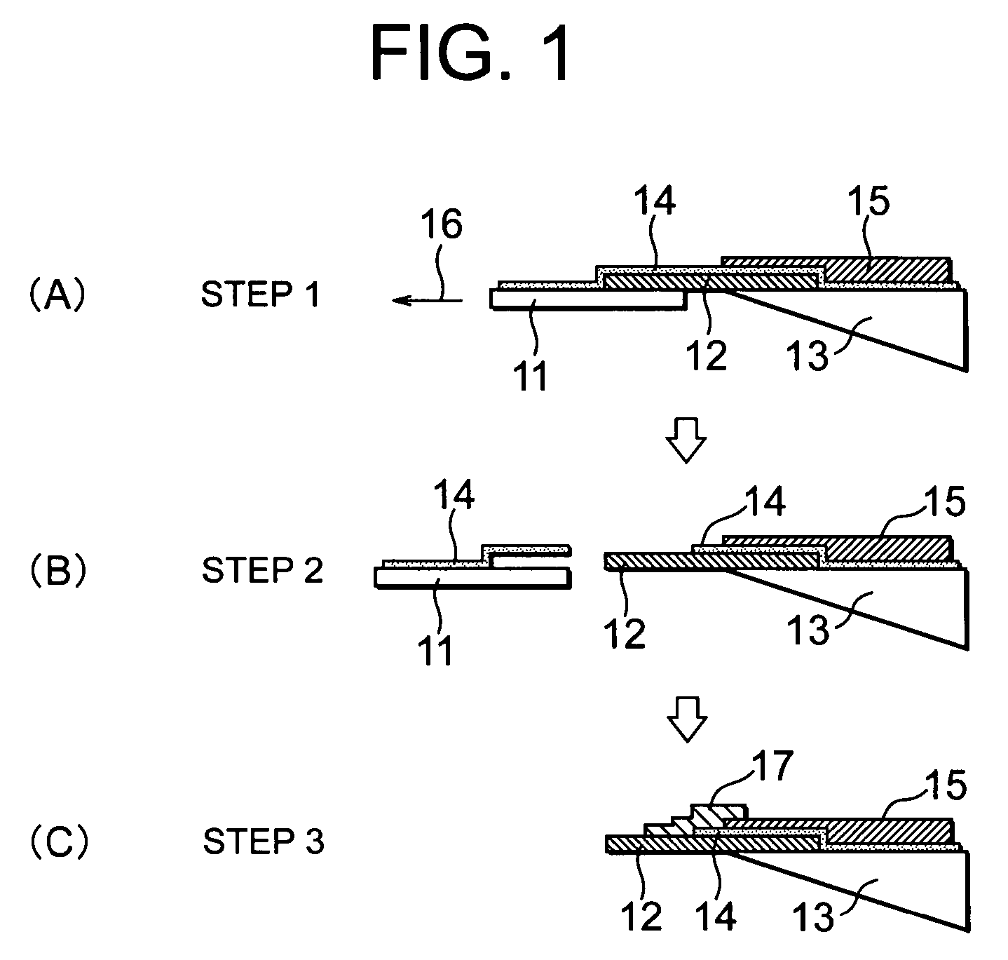
[0038]In the method of producing a probe due to the relationship of the carbon contamination film 14 and bonding coating film 15, a wide region 22 with no coating film is secured. Therefore, when bonding again by the bonding coating film 21 at step 3, the area of the surface of the bonding coating film 21 is increased and the bonding portion is formed including a part in addition to near the end of the mounting base end 13.

[0039]According to the method of producing a probe of the second embodiment, it is possible to increase the region of the exposed part of the carbon nanotube 12, possible to increase the region directly contacting the bonding coating film 21, and possible to improve the bonding strength.

[0040]Referring to FIG. 3, a method of producing a probe according to a third embodiment of the present invention will be explained. In FIG. 3, elements the same as elements explained in FIG. 1 or FIG. 2 are assigned the same reference notations and explanations are omitted. (A) t...

third embodiment

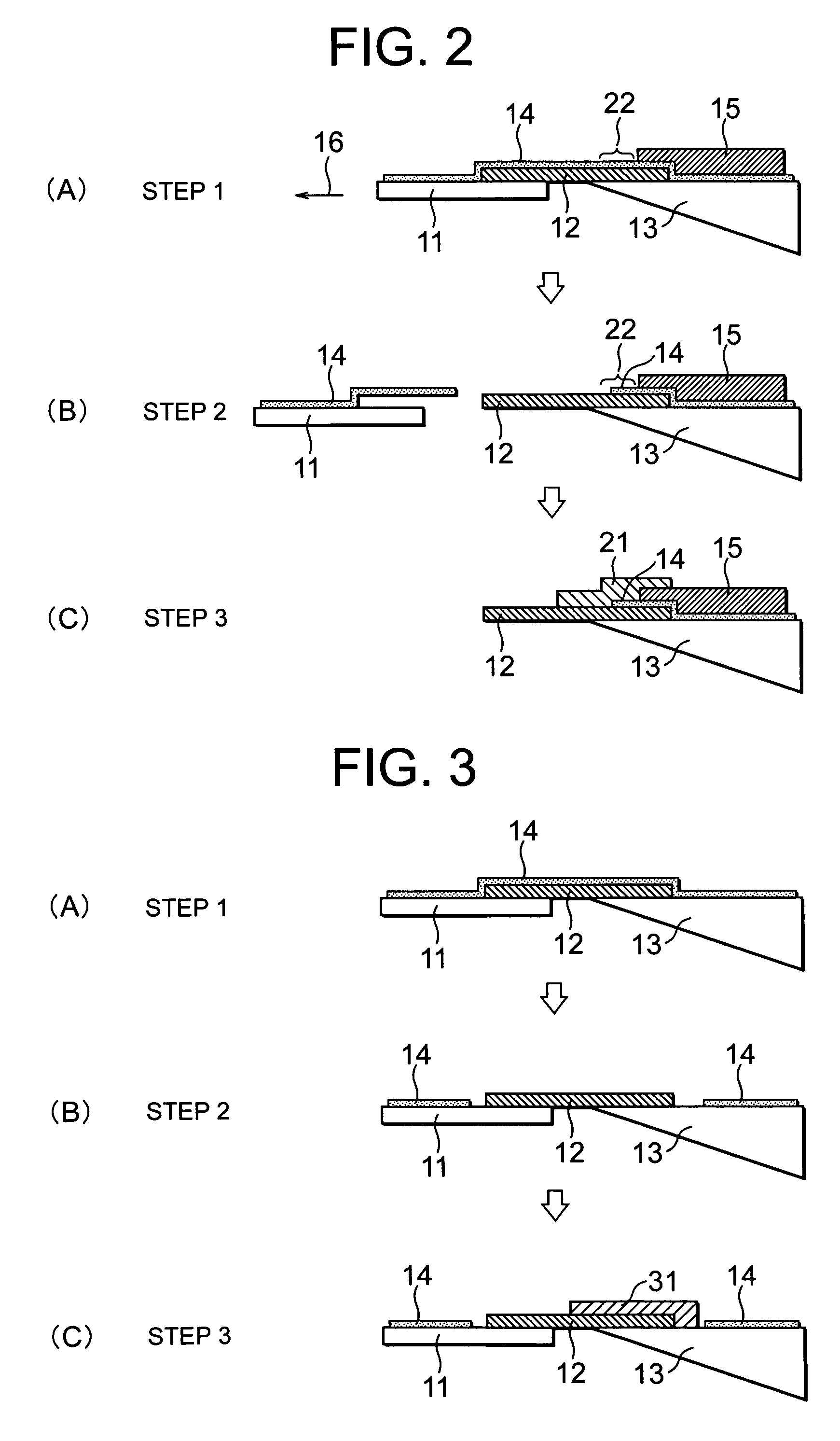
[0041]In the method of producing a probe at step 1, the holder 11 provided with the carbon nanotube 12 is attached to the mounting base end 13. At this time, the holder 11 and carbon nanotube 12 and the mounting base end 13 are bonded by the carbon contamination film 14. In this state, at step 2, before the coating work, part of the carbon contamination film 14 is removed. The carbon contamination film 14 is removed using for example a method using a focused ion beam (FIB) or a method using heating. After this, as shown at step 3, the bonding coating film 31 is formed between the carbon nanotube 12 and the mounting base end 13. After this, at a suitable timing, the holder 11 is removed.

[0042]According to the third embodiment, before the coating work for forming the bonding coating film 31, it is possible to remove part of the carbon contamination film 14 and bring the bonding coating film 31 into direct contact with the carbon nanotube 12, reliably eliminate the effect of the carbo...


PUM

PropertyMeasurementUnit
diameteraaaaaaaaaa
distancesaaaaaaaaaa
distanceaaaaaaaaaa

Abstract

A probe is made by attaching a carbon nanotube 12 to a mounting base end 13, which eliminates the effects of a carbon contamination film, to increase the bonding strength, increase the conductivity of the probe, and strengthen the bonding performance thereof by coating the entire circumference of the nanotube and the base with a coating film, rather than coating just one side. The work of mounting the carbon nanotube and mounting base end are performed under observation by a microscope. Further, the carbon contamination film 14 formed by an electron microscope is stripped off at a stage before bonding by the coating film.

Description

TECHNICAL FIELD[0001]The present invention relates to a method of producing a probe suitable for stably mounting a nanotube at a base member with a sufficient bonding strength in a scanning probe microscope provided with a probe utilizing a carbon nanotube as a probe tip, such a probe, and such a scanning probe microscope.BACKGROUND ART[0002]In recent years, scanning probe microscopes and electron microscopes using carbon nanotubes and other nanotubes as tips of probes have been proposed (Patent Document 1). Nanotubes are utilized in scanning probe microscopes as probe tips provided at the front ends of cantilevers and are utilized in electron microscopes as electron source probes. Patent Document 1 generally discloses a surface signal scan probe for electronic apparatuses and a method of producing the same. Electronic apparatuses include scanning probe microscopes. The probe disclosed in Patent Document 1 is produced utilizing carbon nanotubes and other various types of nanotubes. ...

Claims


Application Information

Patent Timeline
Patent Type & Authority Patents(United States)
IPC IPC(8): G21K7/00G01Q70/12G01Q70/16
CPCB82Y15/00G01Q70/12B82Y35/00
Inventor MORIMOTO, TAKAFUMISHINAKI, TOORUNAG'NO, YOSHIYUKIKENBOU, YUKIOKUNITOMO, YUUICHIHIROKI, TAKENORIKURENUMA, TOORUYANAGIMOTO, HIROAKIKURODA, HIROSHIMIWA, SHIGERUMURAYAMA, KENHAYASHIBARA, MITSUOHIDAKA, KISHIOFUJIEDA, TADASHI
Owner VIVENTIA BIOTECH
Why Eureka
Try Eureka