Electrically pumped Group IV semiconductor micro-ring laser

a semiconductor micro-ring laser and electric pump technology, applied in laser cooling arrangements, laser details, optical resonator shape and construction, etc., can solve the problems of weak vertical confinement of light, not providing definitive lasing,

Inactive Publication Date: 2008-06-24
AIR FORCE US SEC THE
View PDF10 Cites 23 Cited by
  • Summary
  • Abstract
  • Description
  • Claims
  • Application Information

AI Technical Summary

Problems solved by technology

The search for electrically pumped silicon-based lasers that emit light near 1.3 and 1.55 μm telecomm wavelengths has been underway for years, with a diversity of approaches tried including doping silicon with Erbium ions, or using silicon nano-crystals; however, these as well as other approaches have not provided definitive lasing.
This device exhibited stimulated emission at 1.21 μm, however, no resonator was present, the vertical confinement of light was weak, and the ridge was wide.

Method used


Image

  • Electrically pumped Group IV semiconductor micro-ring laser
  • Electrically pumped Group IV semiconductor micro-ring laser
  • Electrically pumped Group IV semiconductor micro-ring laser

Examples


Embodiment Construction

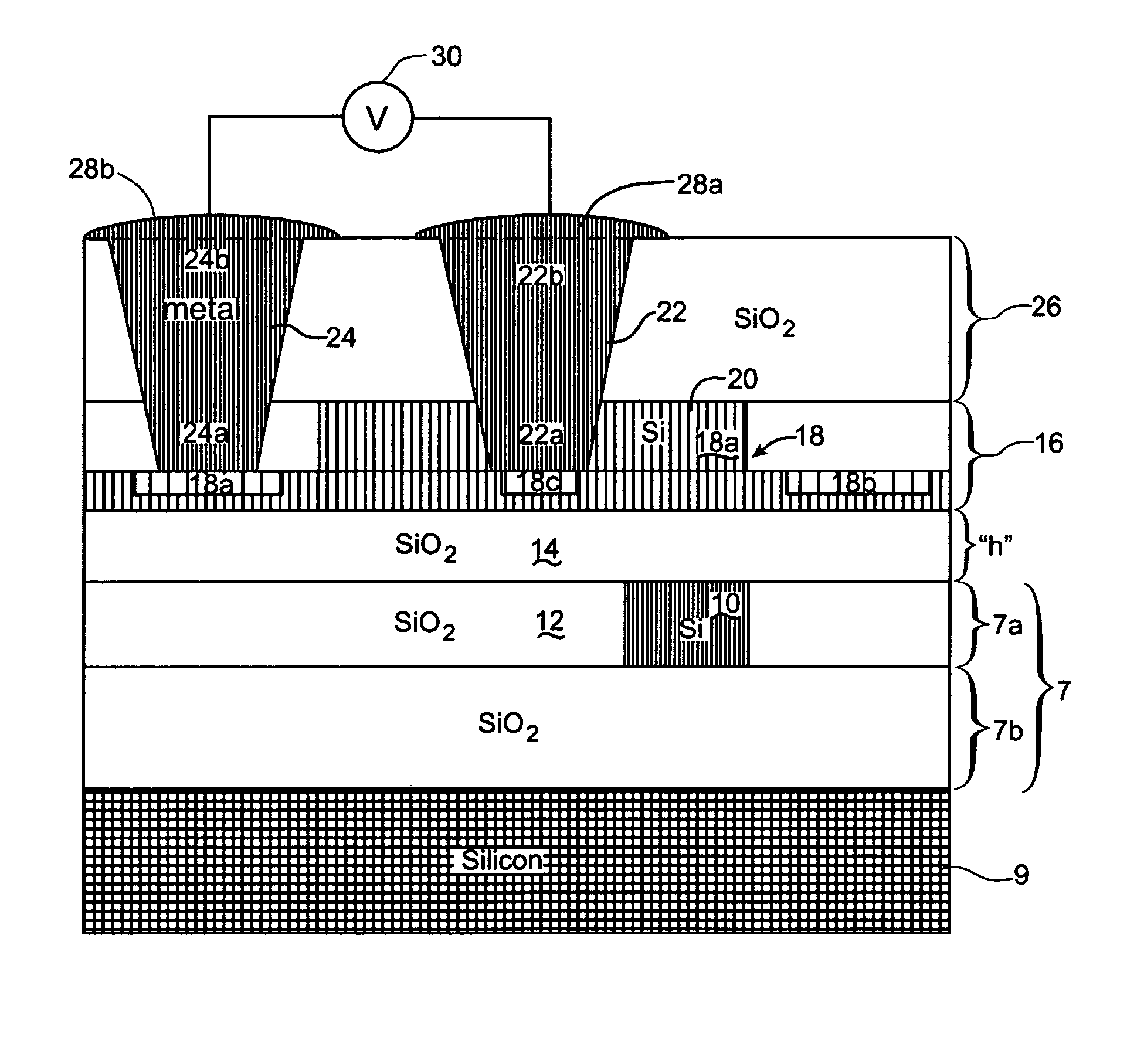
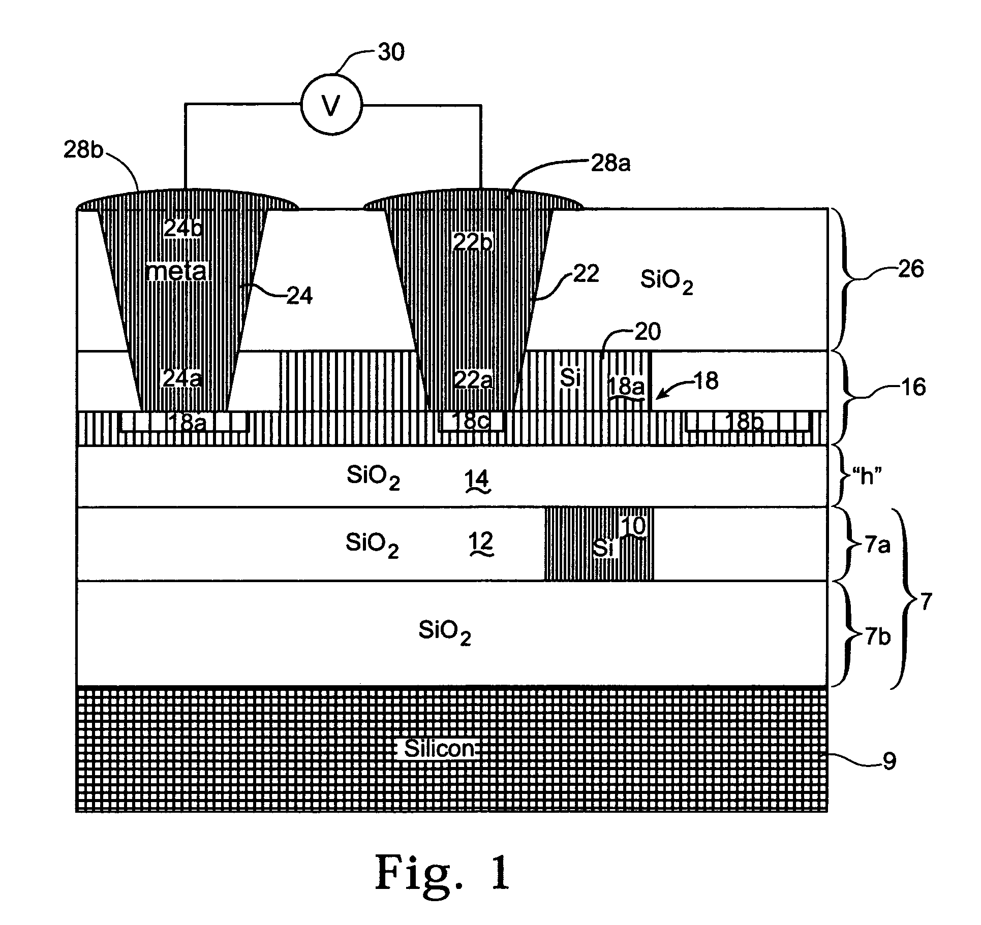
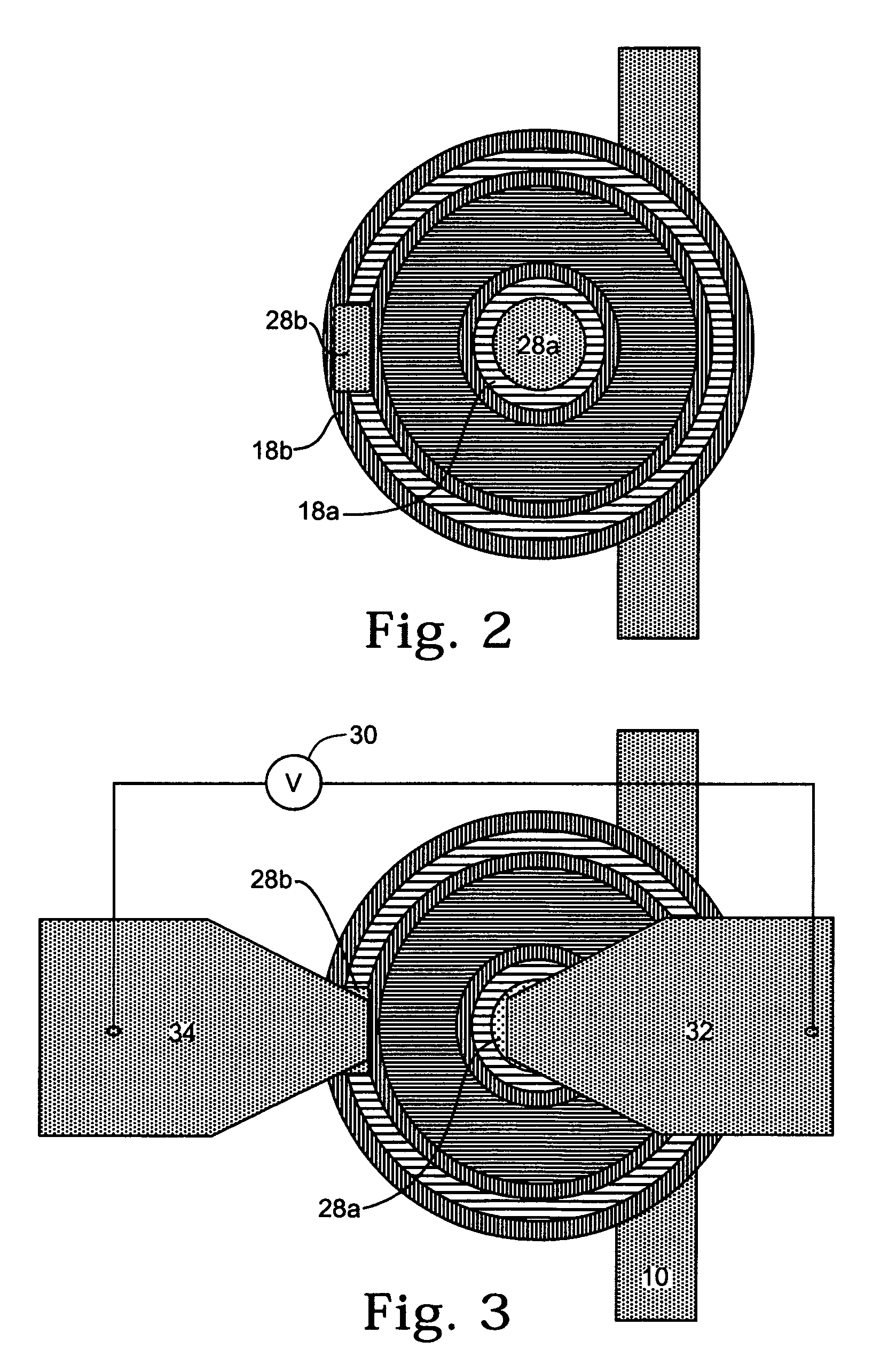
[0013]The present invention provides an electrically pumped silicon-based semiconductor micro-ring laser. The electrically pumped semiconductor micro-ring laser is constructed and arranged to provide a light beam at an optical output of the laser having a wavelength ranging from approximately 1200 nm to approximately 2000 nm, which is particularly useful in telecommunication applications, optical interconnects, optical signaling and / or a number of other computing or signaling applications.

[0014]Referring now to FIG. 1, shown is a cross-sectional view of one embodiment of the electrically pumped semiconductor micro-ring laser 5 in accordance with principles of the present invention. In the illustrative embodiment, the electrically pumped semiconductor micro-ring laser 5 includes a substrate 7, which in the exemplary embodiment may include a silicon-on-insulator (SOI) wafer having a top layer 7a formed of crystal silicon and a bottom buried layer 7b formed of an insulating or dielectr...


PUM


Abstract

An electrically pumped semiconductor laser is provided as including a waveguide structure disposed on the substrate. An optical coupling layer is disposed on the substrate and the waveguide. A resonator layer is disposed on the optical coupling layer and may be adapted to include a photonic crystal lattice having a plurality of substantially cylindrical pores extending downwardly into the resonator layer. An insulating cap layer may be disposed on the resonator layer which operatives to seal the photonic crystal lattice. A first plug filled vias is formed on a central region of the cap layer, which extends downwardly to permit a bottom portion of the first plug to communicate with the photonic crystal lattice. Further, a second plug filled vias is formed on an edge region of the cap layer and extends downwardly to permit a bottom portion of the second plug to communicate with the photonic crystal lattice.

Description

STATEMENT OF GOVERNMENT INTEREST[0001]The invention described herein may be manufactured and used by or for the Government for governmental purposes without the payment of any royalty thereon.FIELD OF THE INVENTION[0002]The present invention relates generally to Group IV semiconductor devices and, more particularly, to an electrically pumped silicon-based semiconductor micro-ring laser.BACKGROUND OF THE INVENTION[0003]As is known, the semiconductor industry has been trying to develop semiconductor lasers using conventional silicon and / or other Group IV semiconductor manufacturing processes. There has also been significant interest in developing the so-called system on a chip (e.g., SOC), which may include analog and digital circuitry, as well as optical networks, which may all contained in a single package on a single silicon chip. In order to realize an active optical-network-on-a-chip, it has become necessary to provide ultracompact silicon lasers. To make SOCs and other optical s...

Claims


Application Information

Patent Timeline
Patent Type & Authority Patents(United States)
IPC IPC(8): H01S3/08H01S5/00
CPCH01S5/026H01S5/1071H01S5/021H01S5/0425H01S5/1032H01S5/2231H01S5/3223H01S5/3224H01S5/04257
Inventor SOREF, RICHARD A.EMELETT, STEPHEN J.
Owner AIR FORCE US SEC THE
Why Eureka
Try Eureka