

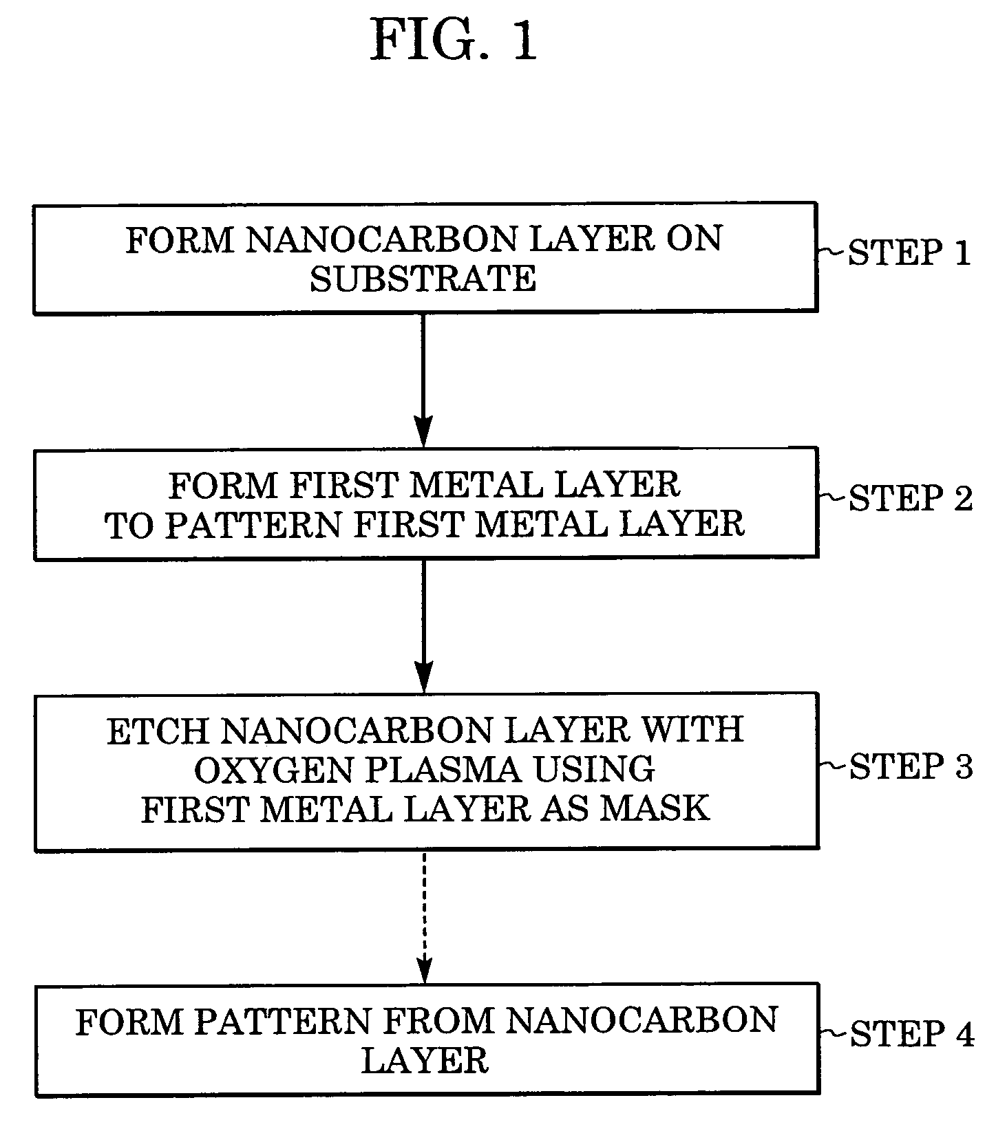
Process for patterning nanocarbon material, semiconductor device, and method for manufacturing semiconductor device
a nanocarbon material and nanotechnology, applied in the manufacture of electrode systems, electric discharge tubes/lamps, printing press parts, etc., can solve the problems of difficult to remove the catalyst layer, and reduce the formation rate of carbon nanotube layers. , to achieve the effect of being ready to manufactur
- Summary
- Abstract
- Description
- Claims
- Application Information
AI Technical Summary
Benefits of technology
Problems solved by technology
Method used
Image

Examples
example 1
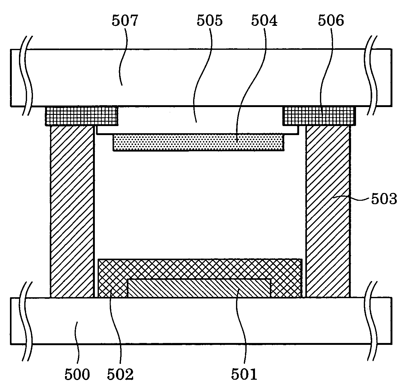
[0078]A wiring pattern was formed by the process of the present invention, whereby an element for measuring the resistance of a wire made of a nanocarbon material was prepared. FIGS. 7A to 7E show steps of preparing the element. With reference to FIGS. 7A to 7E, reference numeral 600 represents an insulating substrate made of Corning 7059 glass, reference numeral 601 represents electrode pads used as measurement terminals, reference numeral 602 represents a nanocarbon layer containing the carbon nanotubes, reference numeral 603 represents a mask layer (first metal layer), and reference numeral 604 represents a photoresist layer.
[0079](1) Magnets were arranged under the rear face of the insulating substrate 600, a Permalloy mask having a negative pattern corresponding to the electrode pads 601 was placed on the front face of the insulating substrate 600, and the electrode pads 601 each including the following layers were formed on the front face of the insulating substrate 600 with a...
example 2-1
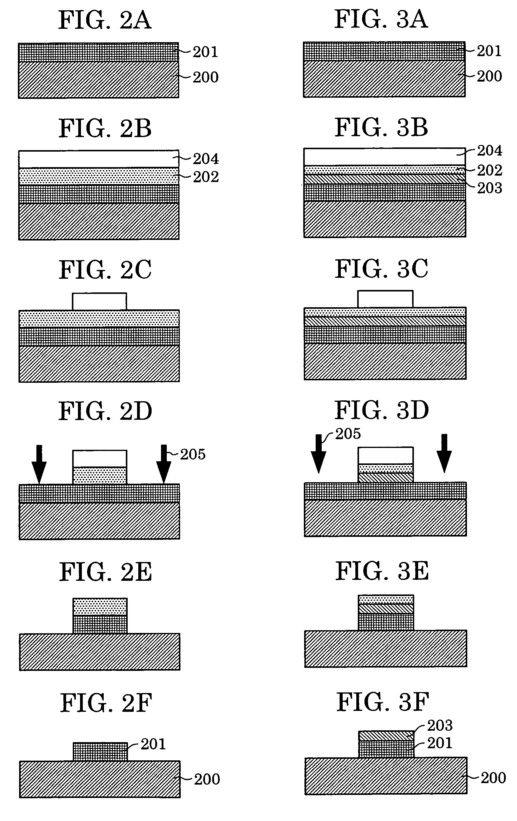
[0085]An element including a nanocarbon wire similar to that shown in FIG. 7E was prepared by the same procedure as that described in Example 1 except that a mask layer 603 of this element included no Cu sub-layer nor Zn sub-layer, but did contain Zn, and had a thickness of 200 nm.
example 2-2
[0086]An element having the same configuration as that described in Example 2-1 was prepared and a mask layer 603 of this element was then etched off with ammonia water.
PUM
| Property | Measurement | Unit |
|---|---|---|
| size | aaaaa | aaaaa |
| temperature | aaaaa | aaaaa |
| temperature | aaaaa | aaaaa |
Abstract
Description
Claims
Application Information