

Photoelectric conversion device and method of manufacturing the device
a technology of conversion device and photoelectric converter, which is applied in the direction of sustainable manufacturing/processing, final product manufacturing, light radiation electric generator, etc., can solve the problems of reduced productivity and degradation of conversion efficiency, and achieve high conversion efficiency, improve adhesion, and improve the effect of adhesion
- Summary
- Abstract
- Description
- Claims
- Application Information
AI Technical Summary
Benefits of technology
Problems solved by technology
Method used
Image

Examples
example 1
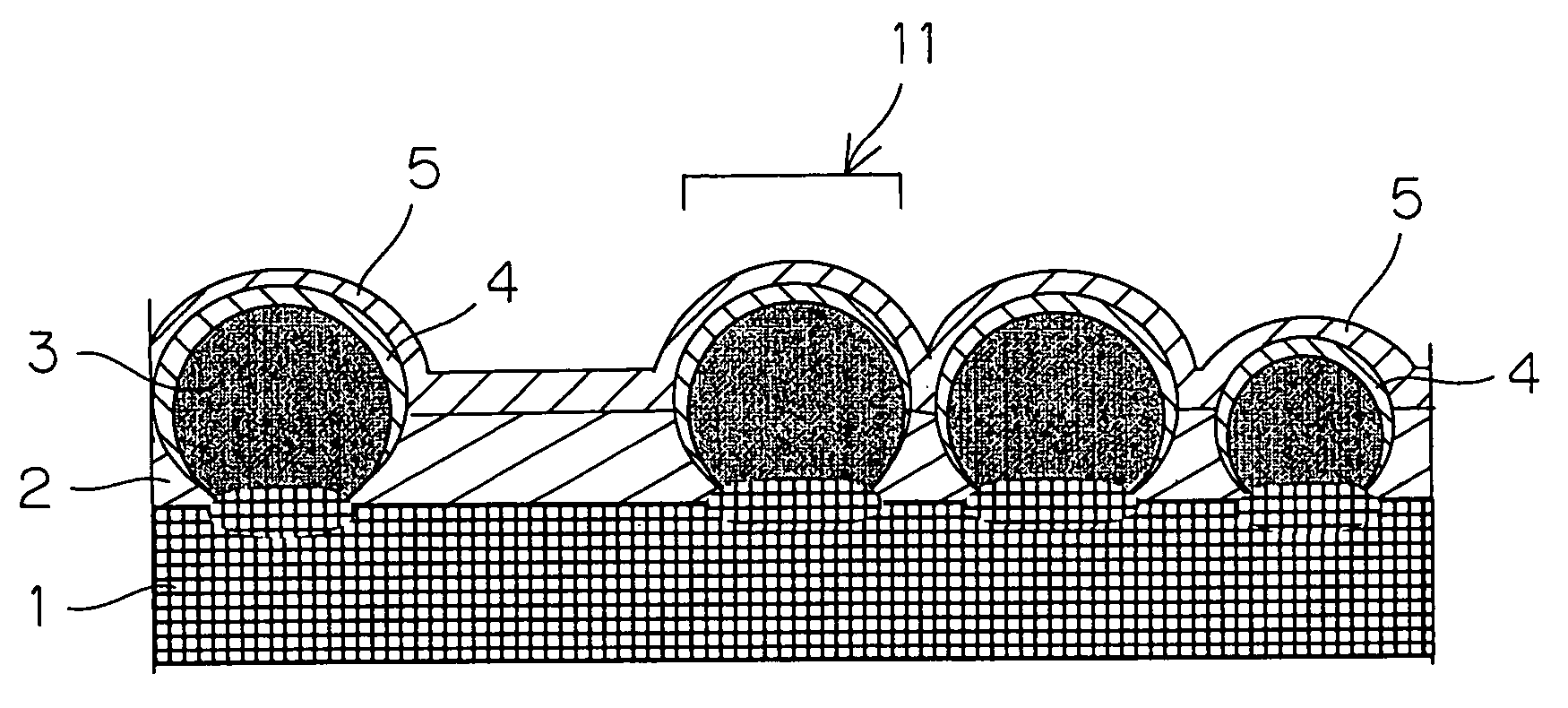
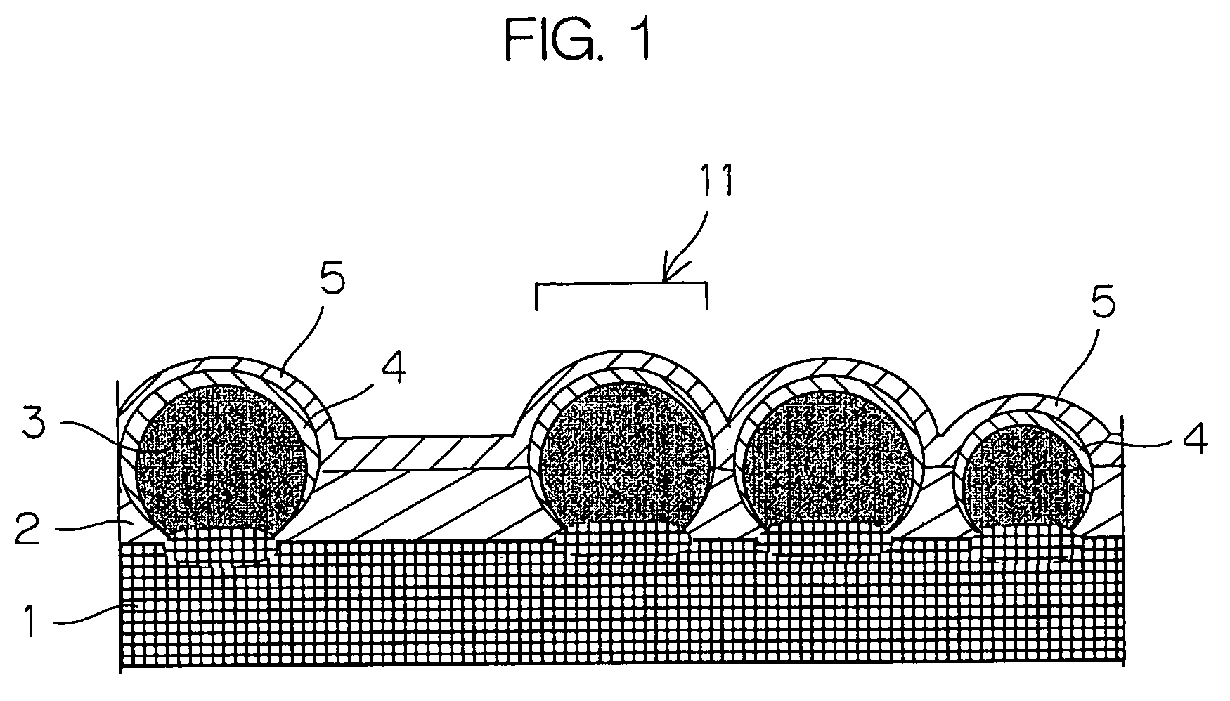
[0076]First, p-type crystalline silicon particles 3 with an average particle size of 400 μm were densely placed to form a layer on an aluminum substrate 1, which were then heated at 590-600° C. so that the crystalline semiconductor particles 3 were joined to the substrate 1.
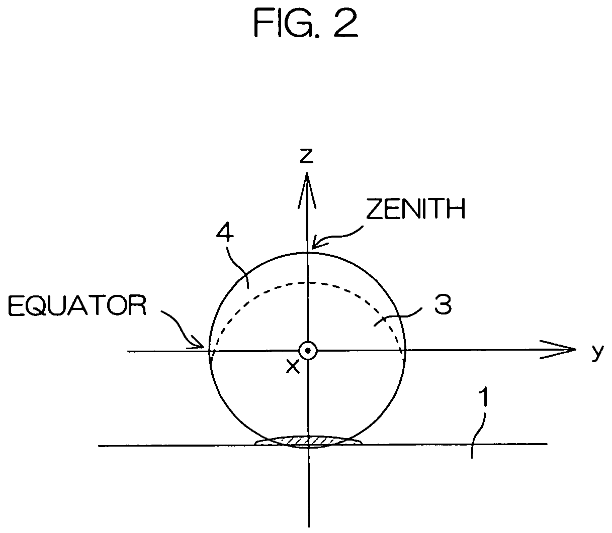
[0077]Subsequently, with a substrate temperature of 250° C., n-type microcrystalline semiconductor layers 4 were formed over the silicon particles 3 from the zenith regions to lower regions thereof by a plasma CVD method. In this process, a pressure in the formation of the layer 4 of 150-300 Pa, and a power of 50-300W was applied to an electrode 12 of the plasma CVD apparatus so that directionality in film growth was caused. As a result, the semiconductor layers 4 each had the largest thickness at the zenith region and a thickness smaller than that at the lower region.
[0078]Then, epoxy resin was provided among the silicon particles 3 and cured to form an insulator layer 2, on which a 100 nm upper electrode layer ...
example 2
[0083]P-type crystalline silicon particles 3 with an average particle size of 400 μm were densely placed to form a layer on an aluminum substrate 1, which were then heated at 590-600° C. so that the crystalline semiconductor particles 3 were joined to the substrate 1.
[0084]Subsequently, with a substrate temperature of 200° C., 40 nm thick, n-type amorphous semiconductor layers 4 were formed by a plasma CVD method. The phosphorus concentration in the semiconductor layers 4 was varied in the direction of thickness by regulating the amount of phosphine gas for doping. Then, epoxy resin was provided among the silicon particles 3 and cured to form an insulator layer 2, on which a 100 nm upper electrode layer 5 comprising ITO was formed. Thereafter, conversion efficiency was measured. Also, with the conditions being the same, a sample device with the surfaces of the crystalline silicon particles 3 being roughened was fabricated and evaluated. In addition, a sample device with the silicon ...
example 3
[0087]P-type crystalline silicon particles 3 with an average particle size of 400 μm were densely placed to form a layer on an aluminum substrate 1, which were then heated at 590-600° C. so that the crystalline semiconductor particles 3 were joined to the substrate 1.
[0088]Subsequently, with a substrate temperature of 150° C., n-type mixed crystal semiconductor layers 4 were formed by a plasma CVD method in which thickness at the zenith regions was varied by controlling the deposition time. Then, polyimide resin was provided among the silicon particles 3 and baked at 200° C. to form an insulator layer 2, on which a 90 nm upper electrode layer 5 comprising ITO was formed. Thereafter, conversion efficiency was measured, the results of which are shown in Table 4.
[0089]
TABLE 4Thickness of n-typeConversionSamplesemiconductor layer 4efficiencyNo.(nm)(%) 31*46.732510.233711.2341011.5353011.4365012.5376011.7388011.93910012.3 40*1108.6 41*1207.1*Samples Nos. 31, 40 and 41 are out of the scop...
PUM
 Abstract
Description
Claims
Application Information