Methods for manufacturing an active matrix display device

a display device and active matrix technology, applied in the direction of semiconductor devices, electrical devices, electric discharge tubes, etc., can solve the problems of impurities having a margin of error, ion beams becoming impossible to be irradiated, etc., to reduce resist degasification and prevent drastic pressure changes

Inactive Publication Date: 2008-07-29
SEMICON ENERGY LAB CO LTD
View PDF11 Cites 0 Cited by
  • Summary
  • Abstract
  • Description
  • Claims
  • Application Information

AI Technical Summary

Benefits of technology

[0009]In view of the foregoing, it is an object of the present invention is to carry out stable doping and to prevent the drastic pressure change in a treatment chamber by reducing degasification of resist during adding impurities.
[0010]In the present invention, the stability of the impurity ion injection is ensured by reducing degasification of resist by reducing the area (resist area proportion, that is, the ratio of the area of resist to the whole area of a substrate) of resist pattern which is used depending on the conditions such as acceleration voltage or current density of a doping process.
[0017]In the above constitution, it is preferable that the area of mask be at most 35% of the area of the substrate in case of reducing the area of the mask. Especially, it produces great effects in case of doping with the acceleration voltage of 80 kV.
[0032]The present invention includes not only the structure that reduces an area of the resist but also that removes previously degasification of resist by heating the substrate before carrying out doping.

Problems solved by technology

However, there are problems that resist which is generally used as a mask is degassed by ion beam irradiation, due to this, pressure in a treatment chamber is increased, and so ion beam becomes impossible to be irradiated, an injection amount of impurities has a margin of error, or the like.

Method used


Image

  • Methods for manufacturing an active matrix display device
  • Methods for manufacturing an active matrix display device
  • Methods for manufacturing an active matrix display device

Examples


embodiment mode 1

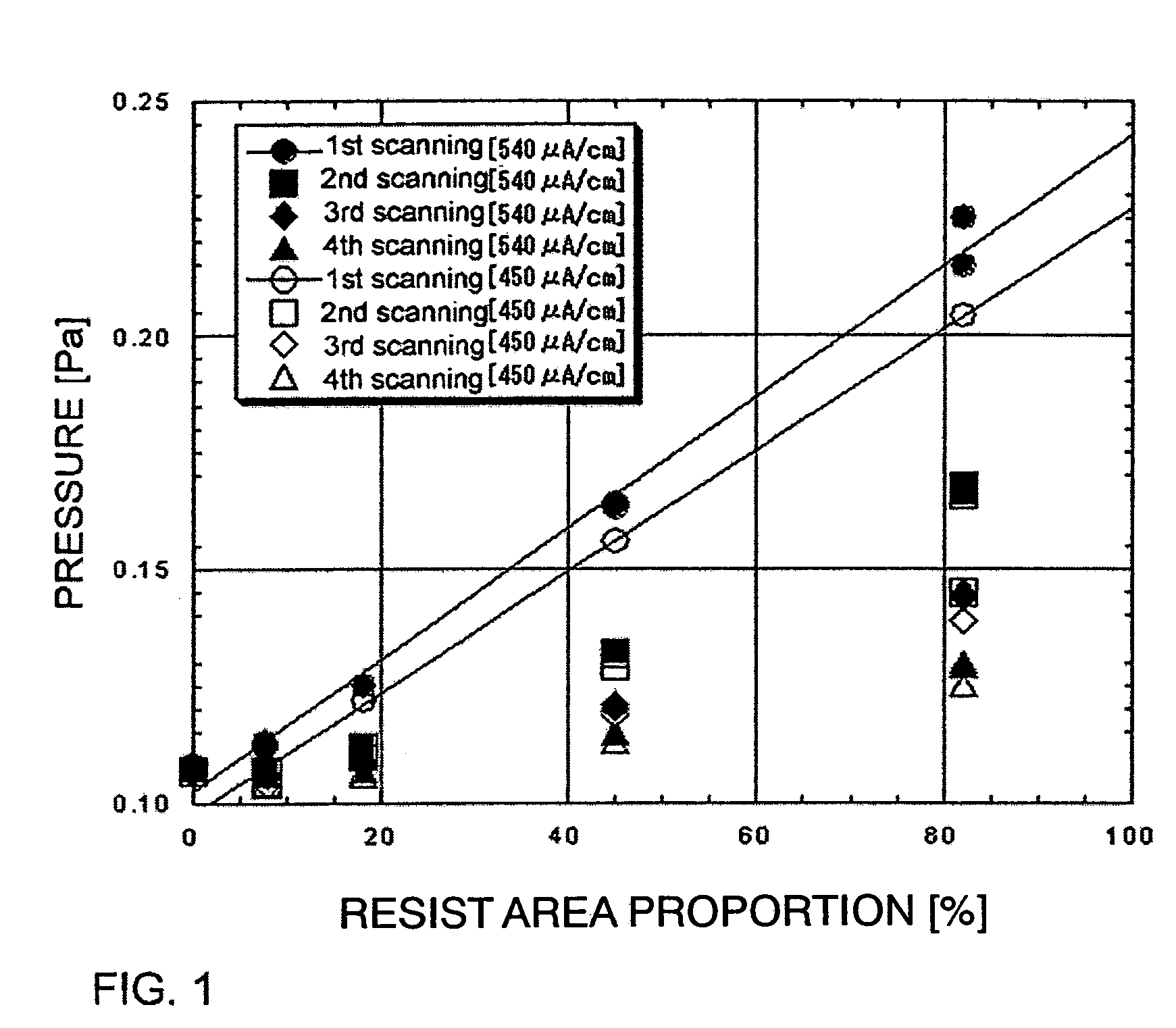
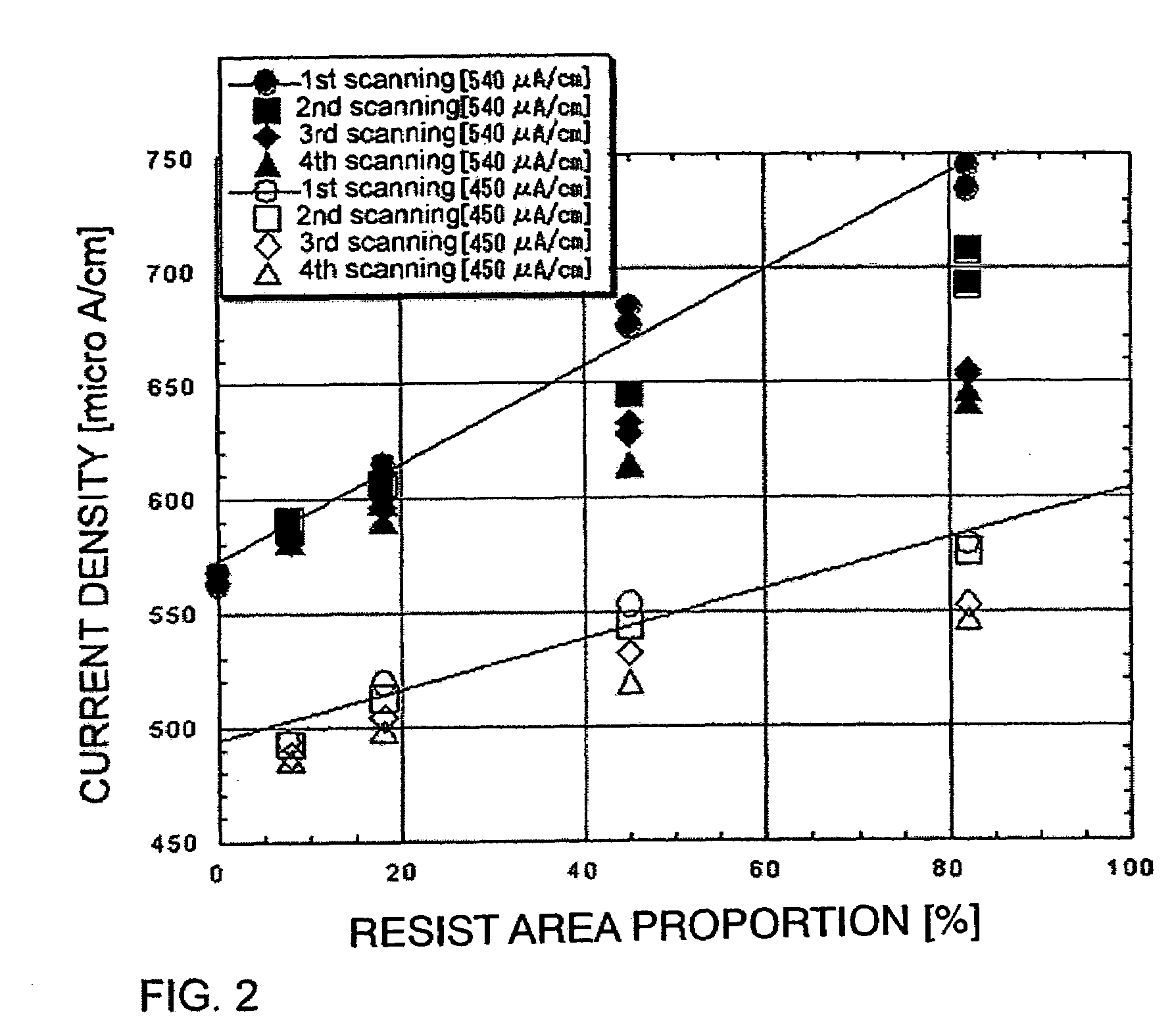
[0070]In Embodiment Mode 1, the results of forming resist patterns each of which has different area proportion over a substrate and implanting ions over a substrate by a doping device. Here, after resists are formed, the resulted resist are heated at 200° C. for 2 hours. The doping device has the structure in which a substrate is scanned at plural times from an ion generator to the position where ions are implanted. Ions are implanted to one position at the same number of times as the number of scanning. Specific structure of the doping device will be described in Embodiment Mode 2, so that explanation thereof is omitted here.

[0071]Firstly, the measurement of the pressure inside a treatment chamber (a doping chamber) during ion implantation gives the results that the pressure inside the treatment chamber is decreased according to decreasing the resist area proportion (%) as shown in FIG. 1 (especially at the first scanning). FIG. 1 shows that the pressure is measured from the first ...

embodiment mode 2

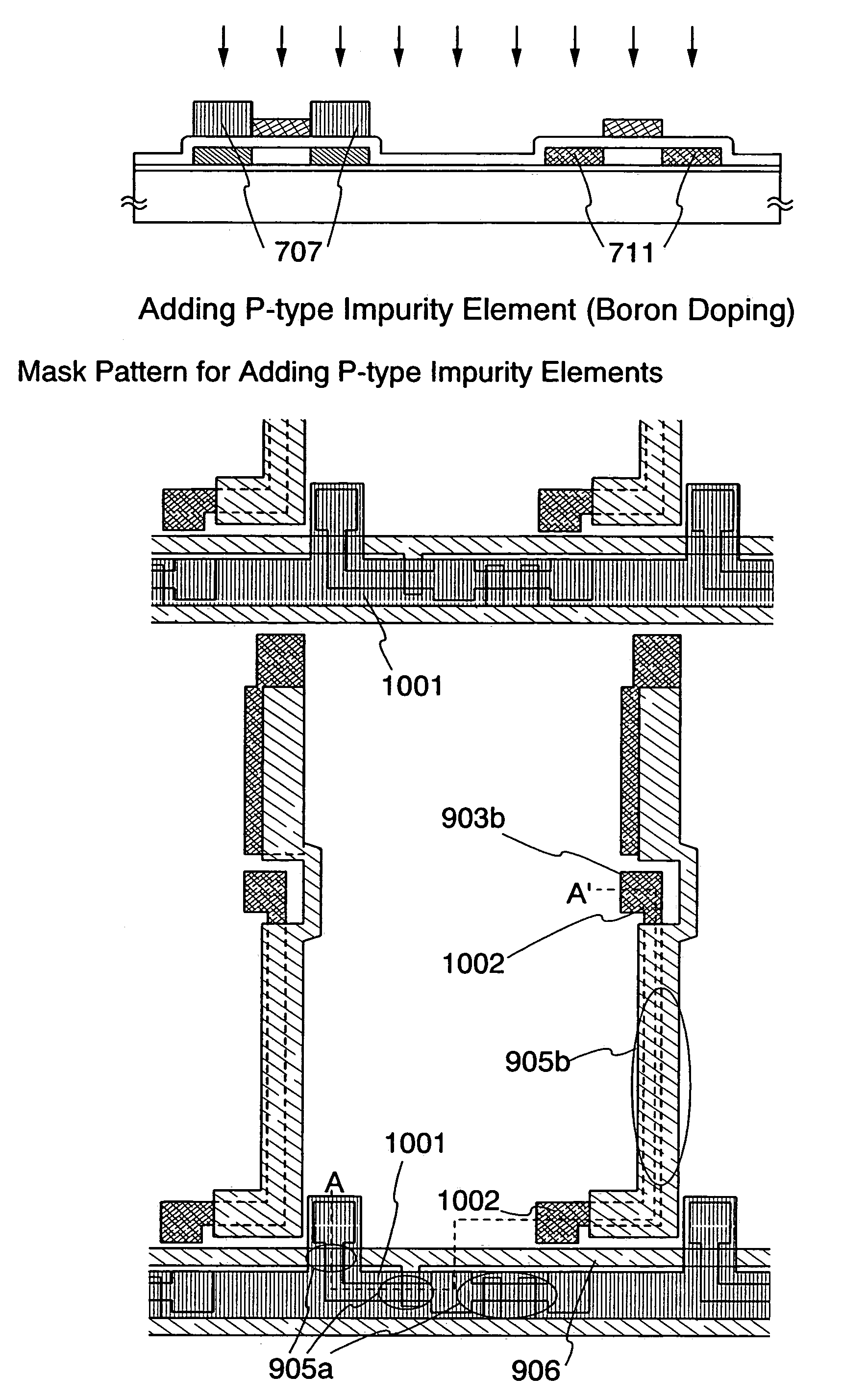
[0079]In this embodiment mode, a method for doping according to the present invention will be described. The case that n-type impurity elements and p-type impurity elements are added respectively to one substrate by doping method using resist with minimal area proportions as a mask will be described.

[0080]In FIG. 7A, a base film 702 is formed to have a thickness of from 50 to 200 nm, which is formed of one kind or plural kinds selected from the group consisting of silicon nitride, silicon oxide, or silicon oxynitride, over a substrate 701 formed of glass, such as barium borosilicate glass or aluminum borosilicate, quartz, or the like, and semiconductor films 703a, 703b having shapes of islands are formed over the base film 702. In the present invention, a silicon substrate can be used for the substrate 701.

[0081]Next, a gate insulating film 704 is formed to have a thickness of 80 nm. The gate insulating film 704 is formed by plasma CVD or sputtering. A silicon oxynitride film formed...

embodiment mode 3

[0091]A doping device used in the present invention will be described reference to FIG. 8 in this embodiment mode. FIG. 8A is a view showing a top-surface of the doping device. FIG. 8B is a cross-sectional view of a doping chamber included in the doping device.

[0092]Main constitutions of the doping device are: a treatment chamber 802 having ion source 801; a load lock chamber (1) 803; a load lock chamber (2) 804; a transporting chamber 805; and an air displacement pump 806. The treatment chamber 802 is a place for infecting ion while moving alternately a substrate in the direction of the arrow shown in FIG. 8A and has a substrate stage 807 and a pressure gauge 808.

[0093]Transportation of a substrate is start from the load lock chambers (1) 803 and (2) 804 into the treatment chamber 802 by an arm 810 provided with the transporting chamber 805, or start from the treatment chamber 802 into the load lock chambers (1) 803 and (2) 804.

[0094]The treatment chamber 802 and the transporting c...


PUM


Abstract

The present invention is to carry out stable doping and to prevent the drastic pressure change in a treatment chamber by reducing degasification of resist during adding impurities. In the present invention, the stability of the impurity ion injection can be ensured by reducing degasification of resist by reducing the area (resist area proportion, that is, the ratio of the area of resist to the whole area of a substrate) of resist pattern which is used depending on the conditions such as acceleration voltage or current density of a doping process.

Description

BACKGROUND OF THE INVENTION[0001]1. Field of the Invention[0002]The present invention relates to a method for manufacturing a semiconductor apparatus. More specifically the present invention relates to technique for adding conductive impurities to a semiconductor over a substrate.[0003]2. Related Art[0004]In case of forming an impurity region such as a source or a drain region that is a component of a thin film transistor (TFT), various methods for adding impurities are adopted.[0005]As a method for adding impurities, for example, ion implantation, ion doping, or the like is utilized. The ion implantation is the technique, that is, elements such as boron (B), phosphorus (P), or the like is ionized and mass-separated, then, only necessary ions are accelerated by an electric field, and then, doped to a semiconductor such as silicon. The ion doping is the technique, that is, ions are accelerated by an electric field and doped without mass separation.[0006]In case of utilizing such tech...

Claims


Application Information

Patent Timeline
Patent Type & Authority Patents(United States)
IPC IPC(8): H01L21/00H01L21/027H01L21/266H01L21/336H01L21/77H01L21/84H01L27/12H01L29/786
CPCH01L21/266H01L27/1288H01L29/66757H01L27/1214H01J2237/31711H01L27/127
Inventor USHITANI, HITOMINAGAO, SHOUIWABUCHI, TOMOYUKI
Owner SEMICON ENERGY LAB CO LTD
Why Eureka
Try Eureka