

Process for forming metal layers
a metal layer and process technology, applied in the direction of resistive material coating, metallic material coating process, chemical vapor deposition coating, etc., can solve the problem of generating a plurality of pinhole defects, unable to meet the requirement for further thickness reduction, and unable to achieve the effect of uniform electrical conductivity and high level of smoothness
- Summary
- Abstract
- Description
- Claims
- Application Information
AI Technical Summary
Benefits of technology
Problems solved by technology
Method used
Image

Examples
examples
[0045]As follows, a series of examples are presented and used to validate the effects of the present invention.
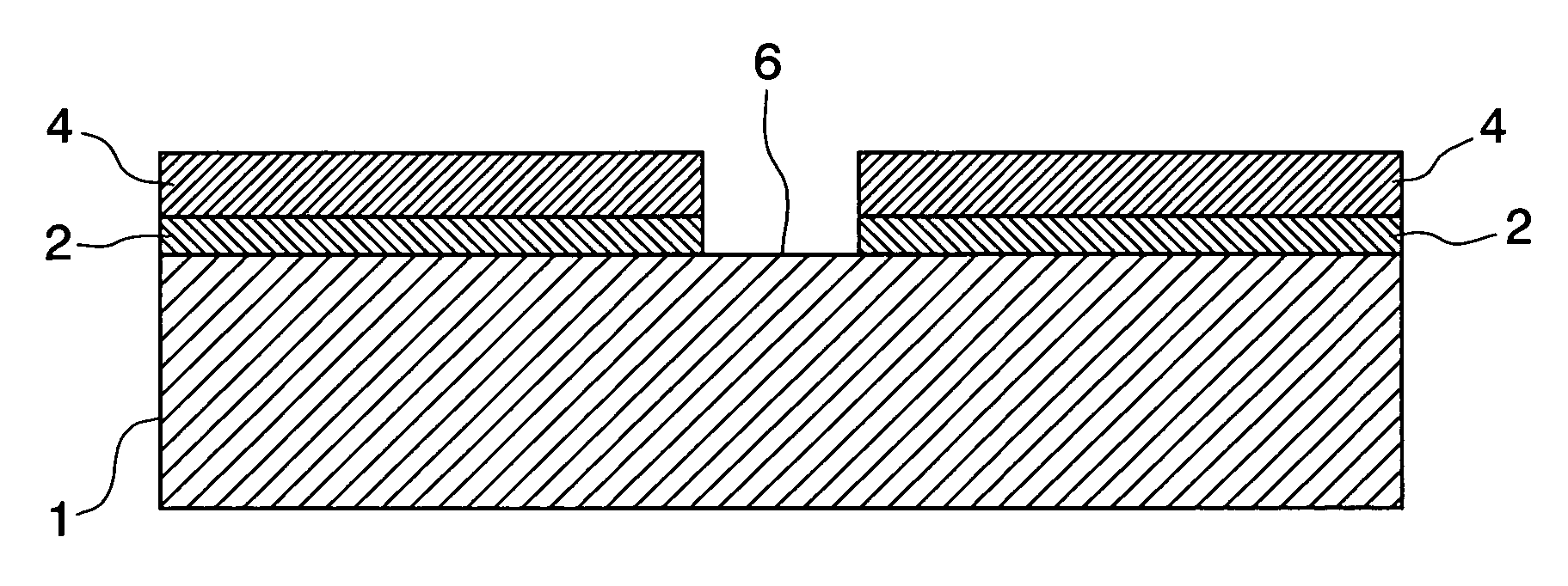
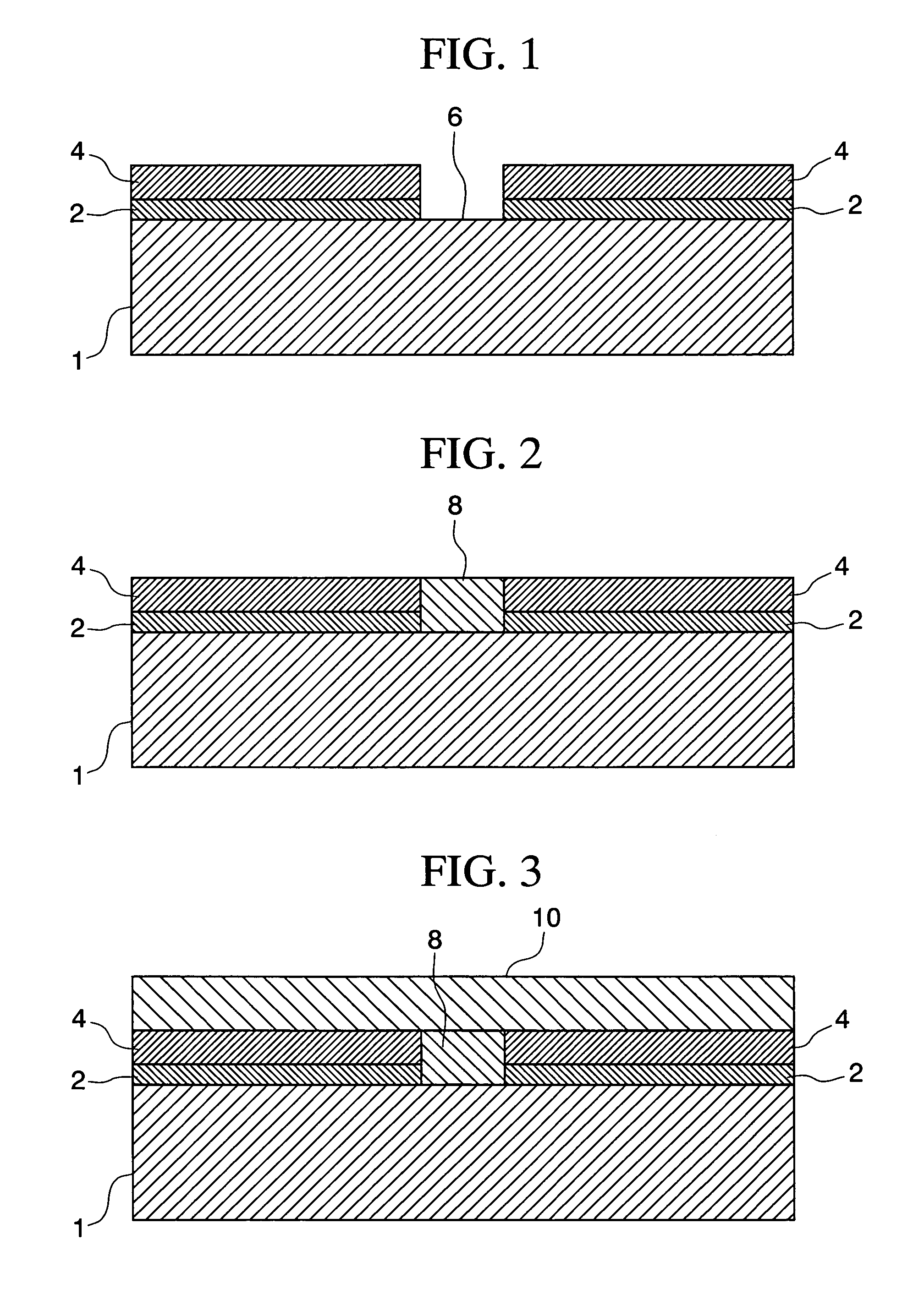
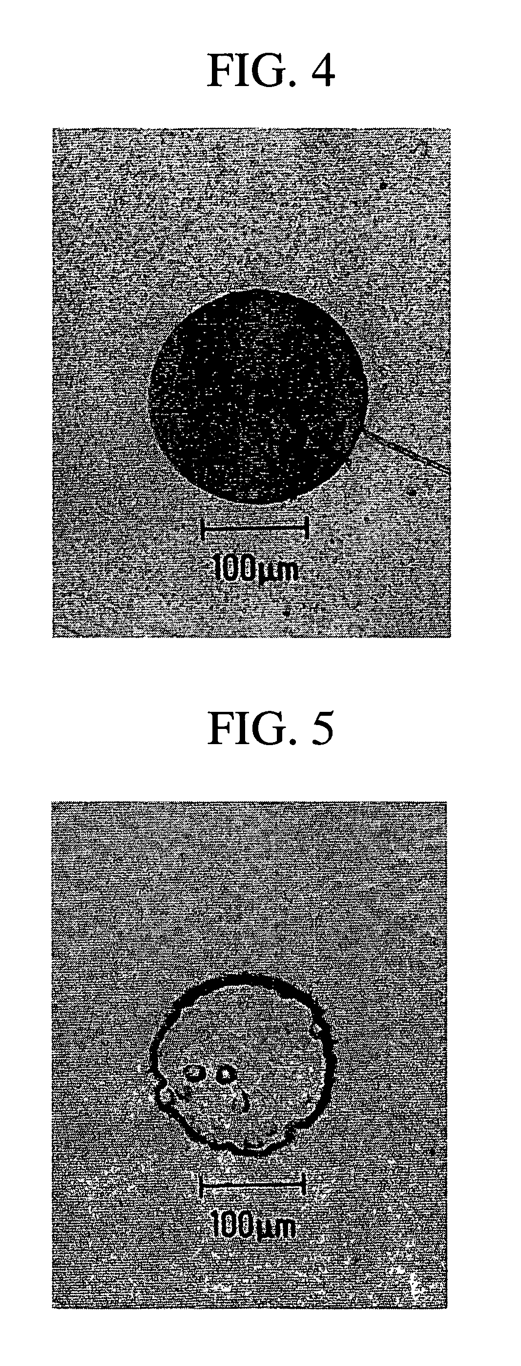
[0046]Vapor deposition was used to deposit 30 mg / m2 of molybdenum on a polyimide film, and a film of copper with a thickness of 300 nm was then deposited by sputtering. An etching treatment was used to form through holes of diameter 200 μm in the copper film, which were treated as pinholes. The polyimide film was then subjected to alkali treatment and a polymer formation treatment, thus forming a conductive organic polymer coating inside the pinholes. Copper sulfate plating was then used to deposit a copper layer on top of the conductive organic polymer coating. The polymer formation treatment was conducted using the procedure and conditions described below.
(1) Degreasing
[0047]The alkali treated film was degreased with an acidic degreasing solution. The acidic degreasing solution was an aqueous solution comprising 50 mL / L of Aktipur AS (a trademark of Enthone Inc.) and 50 m...
PUM
| Property | Measurement | Unit |
|---|---|---|
| thickness | aaaaa | aaaaa |
| sizes | aaaaa | aaaaa |
| thickness | aaaaa | aaaaa |
Abstract
Description
Claims
Application Information