Liquid crystal display driving device of matrix structure type and its driving method

a technology of matrix structure and driving device, which is applied in the direction of instruments, computing, electric digital data processing, etc., can solve the problems of residue image and badly affected image quality, and achieve the effect of increasing the response speed of the liquid crystal display and the aspect ratio of the panel, and reducing the number of data drivers and data lines

Inactive Publication Date: 2008-09-02
ADVANCED IP INNOVATIONS
View PDF5 Cites 12 Cited by
  • Summary
  • Abstract
  • Description
  • Claims
  • Application Information

AI Technical Summary

Benefits of technology

[0012]The chief object of the present invention is to provide a liquid crystal display driving device of matrix structure type to increase the response speed of the liquid crystal display and the aspect ratio of the panel and to decrease the number of the data drivers and the data lines.
[0013]Another object of the present invention is to provide a driving method for the liquid crystal display of matrix structure type, which can simultaneously or synchronously start the plurality of thin film transistors in the display panel and drive the pixels controlled by the thin film transistors to reduce the response time of the liquid crystal display.
[0014]To achieve the above-stated objects of the present invention, the basic structure of the driving device of the present invention includes a group of thin film transistors with matrix array, gate lines connected with the gate drivers and insulated with each other, wherein the gates and the sources of all the thin film transistors are respectively connected with the gate lines and the data lines. The response time of the liquid crystal display can be reduced by the different arrangement design of the gate lines and the data lines and by the different connection location between the gate lines and the gates of the thin film transistors and between the data liens and the sources of the thin film transistors. The gate drivers can be respectively installed on the left side and the right side of the liquid crystal panel and the data drivers can be respectively installed on the upper side and the lower side. The gate driver can be a chip installed on glass or an integrated gate driver circuit installed on glass.

Problems solved by technology

If the response time of the liquid crystal display is longer than the frame interval time, the phenomena of residue image or skip lattice would happen in the screen so that the quality of the image is badly affected.
This would produce the problem of residue image.

Method used


Image

  • Liquid crystal display driving device of matrix structure type and its driving method
  • Liquid crystal display driving device of matrix structure type and its driving method
  • Liquid crystal display driving device of matrix structure type and its driving method

Examples


first embodiment

The First Embodiment

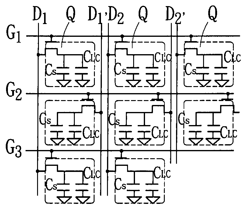
[0072]Referring to FIG. 4A to 4C, they show a preferred embodiment of the liquid crystal display driving device of matrix structure type according to the present invention. The driving device includes a group of thin film transistors Q with matrix array, which consists of N rows and M columns of thin film transistors, wherein, each thin film transistor Q can drive one pixel, so N×M pixels (shown by rectangle with dotted line) can be driven. The first gate line G1 is connected with the gates of all the thin film transistors Q of the first row, the second gate line G2 is connected with the gates of all the thin film transistors Q of the second row, and so are the others. Therefore, there are N gate lines connected to gate driver and they are insulated with each other.

[0073]The first and the second data lines D1, D1′ of the first group of data lines are respectively connected with the sources of all the thin film transistors Q of the odd and the even rows of the fir...

second embodiment

The Second Embodiment

[0079]Referring to FIG. 8A to 8C, the second embodiment of the liquid crystal display driving device of matrix structure type according to the present invention includes a group of thin film transistors with matrix array, which consist of 2N rows and M columns of thin film transistors Q, wherein, each thin film transistor Q can drive one pixel so that 2N×M of pixels (shown by the rectangle with dotted line) can be driven. The first gate line G1 is connected with the gates of all the thin film transistors Q of the first and the second rows, the second gate line G2 is connected with the gates of all the thin film transistors Q of the third and the fourth rows, and so are the others. Therefore, total N gate lines connected to the gate drivers and insulated with each other.

[0080]The first and the second data lines D1, D1′ of the first group of data lines are respectively connected with the sources of all the thin film transistors of the odd rows and the even rows of...

third embodiment

The Third Embodiment

[0088]Referring to FIG. 12A to 12C, the third embodiment of the liquid crystal display driving device of matrix structure type according to the present invention includes a group of thin film transistors with matrix array, which consists of N rows and 2M columns of thin film transistors Q, wherein each thin film transistor can drive one pixel, so total N×2M of pixels (shown by the rectangle of dotted line). The first and the second gate lines G1, G1′ of the first group of the gate lines are respectively connected with the gates of all the thin film transistors of the odd columns and the even columns of the first row, the first and the second gate lines G2, G2′ of the second group of gate lines are respectively connected with the gates of all the transistors Q of the odd columns and the even columns of the second row . . . and the first and the second gate lines of the Nth group of gate lines are respectively connected with the gates of all the thin film transisto...


PUM


Abstract

A liquid crystal display driving device of matrix structure type and its driving method are disclosed in the present invention. The driving device consists of a group of thin film transistors with matrix array, a plurality of gate lines and a plurality of data lines. The object of increasing response speed can be accomplished by the different arrangement of gate lines and data lines and the different connection between each thin film transistor and the gate and data lines. The driving method for the said driving device includes: each pair of gate lines in the display panel are simultaneously and orderly turned on at different time of driving transistor, and the different driving voltages are orderly applied to the thin film transistors connected to the gate lines. The structure and method can suit for picture treating of various displays such as liquid crystal display, organic light-emitting diode (OLED) display or plasma display panel (PDP).

Description

BACKGROUND OF THE INVENTION[0001]1. Field of the Invention[0002]The present invention relates to a liquid crystal display driving device of matrix structure type and its driving method, especially to a display driving device and its driving method, which can simultaneously or synchronously drive a plurality of thin film transistors to increase the response speed, wherein the source and the gate of each thin film transistor in the driving device are respectively connected with different gate lines and data lines to let the specific transistor be driven by the gate drivers and the data drivers, and the predetermined voltage for over drive or the data voltage for the present frame interval is applied to accomplish the object of increasing the response speed. The present invention can suit for the picture treatment of various liquid crystal displays, organic light emitting diode (OLED) display or plasma display panel (PDP).[0003]2. Description of the Prior Art[0004]Because the liquid cr...

Claims


Application Information

Patent Timeline
Patent Type & Authority Patents(United States)
IPC IPC(8): G09G3/36
CPCG09G3/3659G09G2300/0426G09G2300/0814G09G2320/0261G09G2310/0251G09G2310/0297G09G2320/0252G09G2310/0205
Inventor YUH-REN, SHENCHENG-JUNG, CHENCHUN-CHI, CHEN
Owner ADVANCED IP INNOVATIONS
Why Eureka
Try Eureka