Ruthenium containing layer deposition method

a technology of ruthenium containing and layer deposition, which is applied in the direction of coating, chemical vapor deposition coating, metallic material coating process, etc., can solve the problems of dielectric layer becoming conductive, copper diffusing into neighboring layers, and electronic devices failing to work properly

Active Publication Date: 2008-10-21
APPLIED MATERIALS INC
View PDF66 Cites 45 Cited by
  • Summary
  • Abstract
  • Description
  • Claims
  • Application Information

AI Technical Summary

Problems solved by technology

Although copper is a popular interconnect material, copper suffers by diffusing into neighboring layers, such as dielectric layers.
The resulting and undesirable presence of copper causes dielectric layers to become conductive and electronic devices to fail.
Tantalum nitride does have some negative characteristics, which include poor adhesion to the copper layer deposited thereon.
Poor adhesion of the subsequent deposited copper layer(s) can lead to rapid electromigration in the formed device and possibly process contamination issues in subsequent processing steps, such as, chemical mechanical polishing (CMP).
The carbon incorporation is often detrimental to the completion of wet chemical processes since the deposited film tends to be hydrophobic which reduces or prevents the fluid from wetting and depositing a layer having desirable properties.
To solve this problem, oxidizing processes are often used on barrier layers to remove the incorporated carbon, but these processes can have a detrimental effect on the other exposed and highly oxidizable layers, such as, copper interconnects.

Method used


Image

  • Ruthenium containing layer deposition method
  • Ruthenium containing layer deposition method
  • Ruthenium containing layer deposition method

Examples


Embodiment Construction

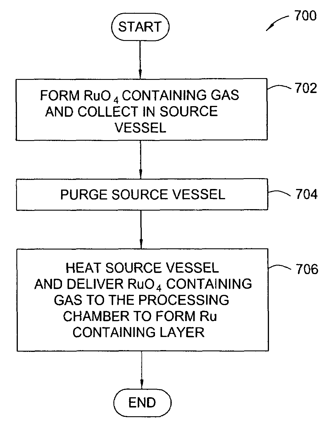
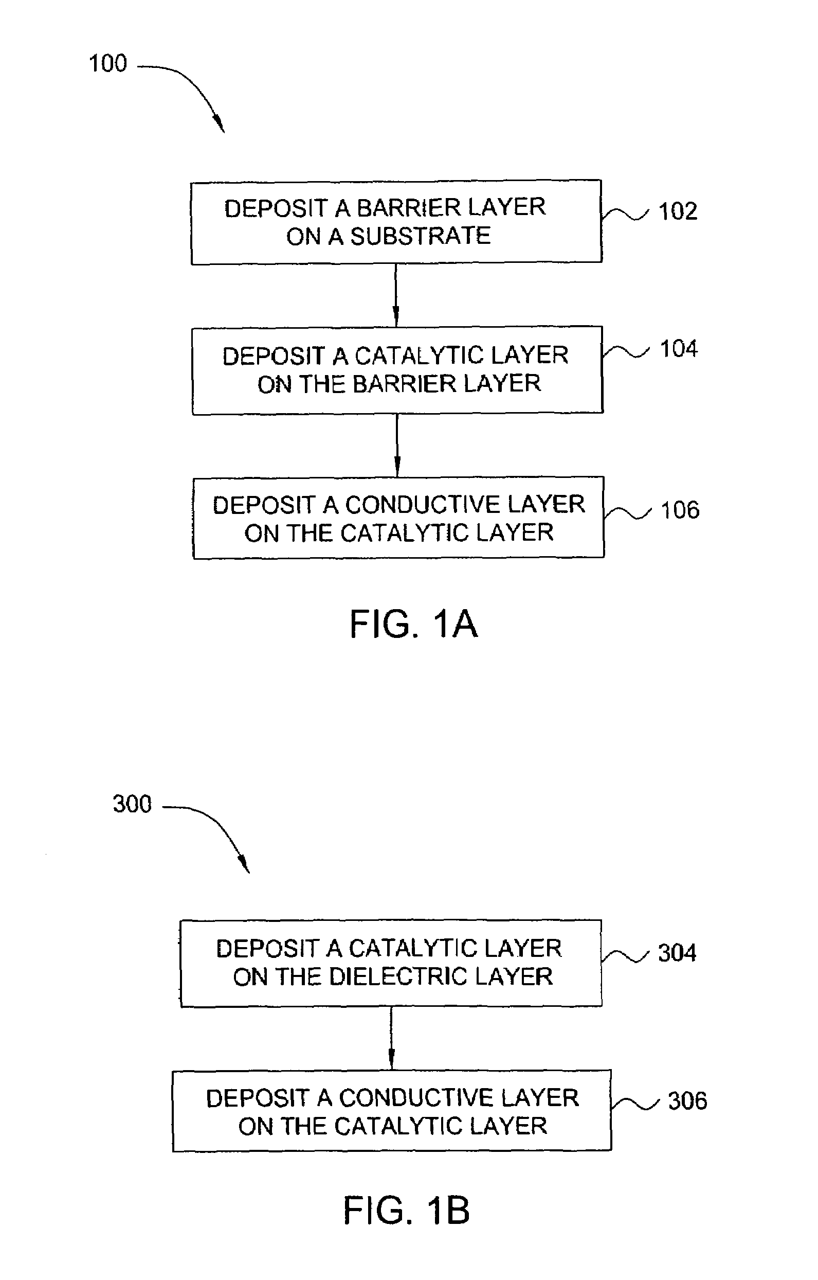
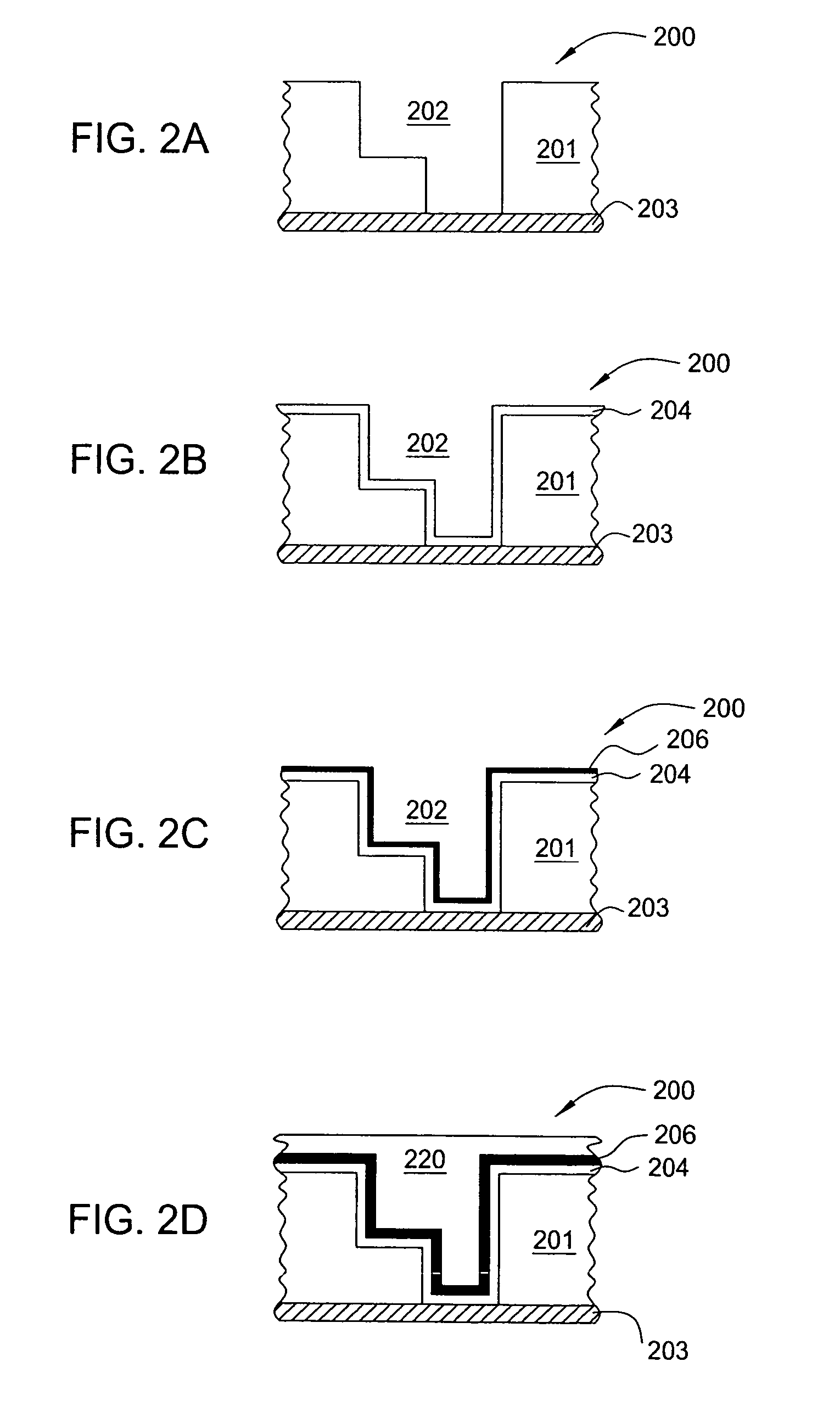
[0032]A method and apparatus for depositing a ruthenium containing layer on a substrate is generally disclosed. The method and apparatus described herein may be especially useful for fabricating electronic devices that are formed on a surface of the substrate or wafer. Generally, the method includes exposing a surface of a substrate to a ruthenium tetroxide vapor to form a catalytic layer on the surface of a substrate and then filling the device structures by an electroless, electroplating, physical vapor deposition (PVD), chemical vapor deposition (CVD), plasma enhanced CVD (PECVD), atomic layer deposition (ALD) or plasma enhanced ALD (PE-ALD) processes. In one aspect, the catalytic layer is a ruthenium containing layer that is adapted to act as a layer that can promote the adhesion between prior and subsequently deposited layers, act as a barrier layer or act as a catalytic layer to promote subsequent PVD, CVD, PECVD, ALD, PE-ALD, electroless and / or electrolytic deposition process...


PUM

PropertyMeasurementUnit
temperatureaaaaaaaaaa

Abstract

An exemplary apparatus and method of forming a ruthenium tetroxide containing gas to form a ruthenium containing layer on a surface of a substrate is described herein. The method and apparatus described herein may be especially useful for fabricating electronic devices that are formed on a surface of the substrate or wafer. Generally, the method includes exposing a surface of a substrate to a ruthenium tetroxide vapor to form a catalytic layer on the surface of a substrate and then filling the device structures by an electroless, electroplating, physical vapor deposition (PVD), chemical vapor deposition (CVD), plasma enhanced CVD (PECVD), atomic layer deposition (ALD) or plasma enhanced ALD (PE-ALD) processes. In one embodiment, the ruthenium containing layer is formed on a surface of a substrate by creating ruthenium tetroxide in an external vessel and then delivering the generated ruthenium tetroxide gas to a surface of a temperature controlled substrate positioned in a processing chamber. In one embodiment, a ruthenium tetroxide containing solvent formation process is used to form ruthenium tetroxide using a ruthenium tetroxide containing source material. In one embodiment, of a ruthenium containing layer is formed on a surface of a substrate, using the ruthenium tetroxide containing solvent. In another embodiment, the solvent is separated from the ruthenium tetroxide containing solvent mixture and the remaining ruthenium tetroxide is used to form a ruthenium containing layer on the surface of a substrate.

Description

CROSS-REFERENCE TO RELATED APPLICATIONS[0001]This application claims the benefit of U.S. Provisional Patent Application Ser. No. 60 / 648,004, filed Jan. 27, 2005 and U.S. Provisional Patent Application No. 60 / 715,024, filed Sep. 8, 2005, which are both herein incorporated by reference.BACKGROUND OF THE INVENTION[0002]1. Field of the Invention[0003]Embodiments of the invention generally relate to methods for depositing a catalytic layer on a barrier layer, prior to depositing a conductive layer thereon.[0004]2. Description of the Related Art[0005]Multilevel, 45 nm node metallization is one of the key technologies for the next generation of very large scale integration (VLSI). The multilevel interconnects that lie at the heart of this technology possess high aspect ratio features, including contacts, vias, lines and other apertures. Reliable formation of these features is very important for the success of VLSI and the continued effort to increase quality and circuit density on individu...

Claims


Application Information

Patent Timeline
Patent Type & Authority Patents(United States)
IPC IPC(8): C23C16/06
CPCC23C16/06C23C16/4488C23C16/45525C23C16/45536C23C16/45544C23C16/5096H01L21/28562H01L21/76843H01L21/76873
Inventor WEIDMAN, TIMOTHY W.
Owner APPLIED MATERIALS INC
Why Eureka
Try Eureka