

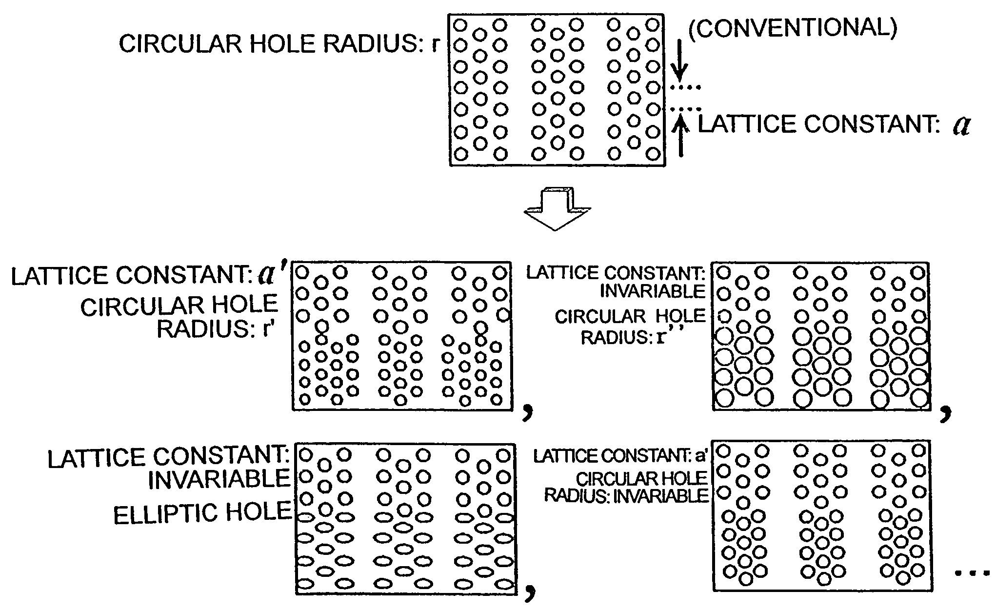
Photonic crystal coupling defect waveguide
a coupling defect waveguide and photonic crystal technology, applied in the direction of optical waveguide light guides, instruments, etc., can solve the problems of difficult to form directional couplers, difficult to alter the coupling length in the middle of propagation, and change to be shorter, so as to shorten the coupling length and the effect of coupling length
- Summary
- Abstract
- Description
- Claims
- Application Information
AI Technical Summary
Benefits of technology
Problems solved by technology
Method used
Image

Examples
example 1
[0163]When heat is applied to a polymer medium by a heater or laser irradiation, the medium constant is changed by the temperature change. A silica-based or polymer-based material is an example having a thermooptic effect.
example 2
[0164]When a DC electric field is applied to LiNbO3 medium, the medium constant is changed. LiNbO3 is one of typical media having the electrooptic effect.
example 3
[0165]When a DC electric field is applied to a structure made of plural compound semiconductors in which the compositions are changed and a current is injected, the medium constant is changed. For example, the compound semiconductor such as GaAs or InP is made to have a laminate structure while the composition is changed little by little, and when the DC electric field is applied vertically to the laminate surface, the medium constant of the structure is changed. This is based on, for example, a carrier effect.
PUM
| Property | Measurement | Unit |
|---|---|---|
| frequency | aaaaa | aaaaa |
| frequency | aaaaa | aaaaa |
| refractive index | aaaaa | aaaaa |
Abstract
Description
Claims
Application Information