
Graphene film as transparent and electrically conducting material

a graphene film, transparent technology, applied in the direction of non-metal conductors, conductors, metal/alloy conductors, etc., can solve the problems of high-temperature sputtering, inability to achieve the right combination of sheet conductance and transparency, and the indium component of ito is rapidly becoming a scarce commodity

Active Publication Date: 2008-11-11
SAMSUNG ELECTRONICS CO LTD
View PDF4 Cites 53 Cited by
  • Summary
  • Abstract
  • Description
  • Claims
  • Application Information

AI Technical Summary

Benefits of technology

The present invention is about a new type of transparent and electrically conducting material made up of small sheets of graphene. These sheets can be combined with other nanostructured materials, like carbon nanotubes, to create even more complex and functional networks. The invention also includes new methods for depositing graphene films onto different substrates. The graphene films can be used to create new devices and integrating them into existing systems. Overall, the invention provides a way to create highly conductive and transparent networks using graphene.

Problems solved by technology

However, ITO can be an inadequate solution for many of the above-mentioned applications (e.g., due to its relatively brittle nature and correspondingly inferior flexibility and abrasion resistance), and the indium component of ITO is rapidly becoming a scarce commodity.
Additionally, ITO deposition usually requires expensive, high-temperature sputtering, which can be incompatible with many device process flows.
However, although nanotube networks fabricated to date are both conducting and transparent, they have not been able to achieve the right combination of sheet conductance and transparency to be competitive with currently used materials such as indium-tin-oxide (ITO).

Method used


Image

  • Graphene film as transparent and electrically conducting material
  • Graphene film as transparent and electrically conducting material
  • Graphene film as transparent and electrically conducting material

Examples


first embodiment

Graphene Flakes

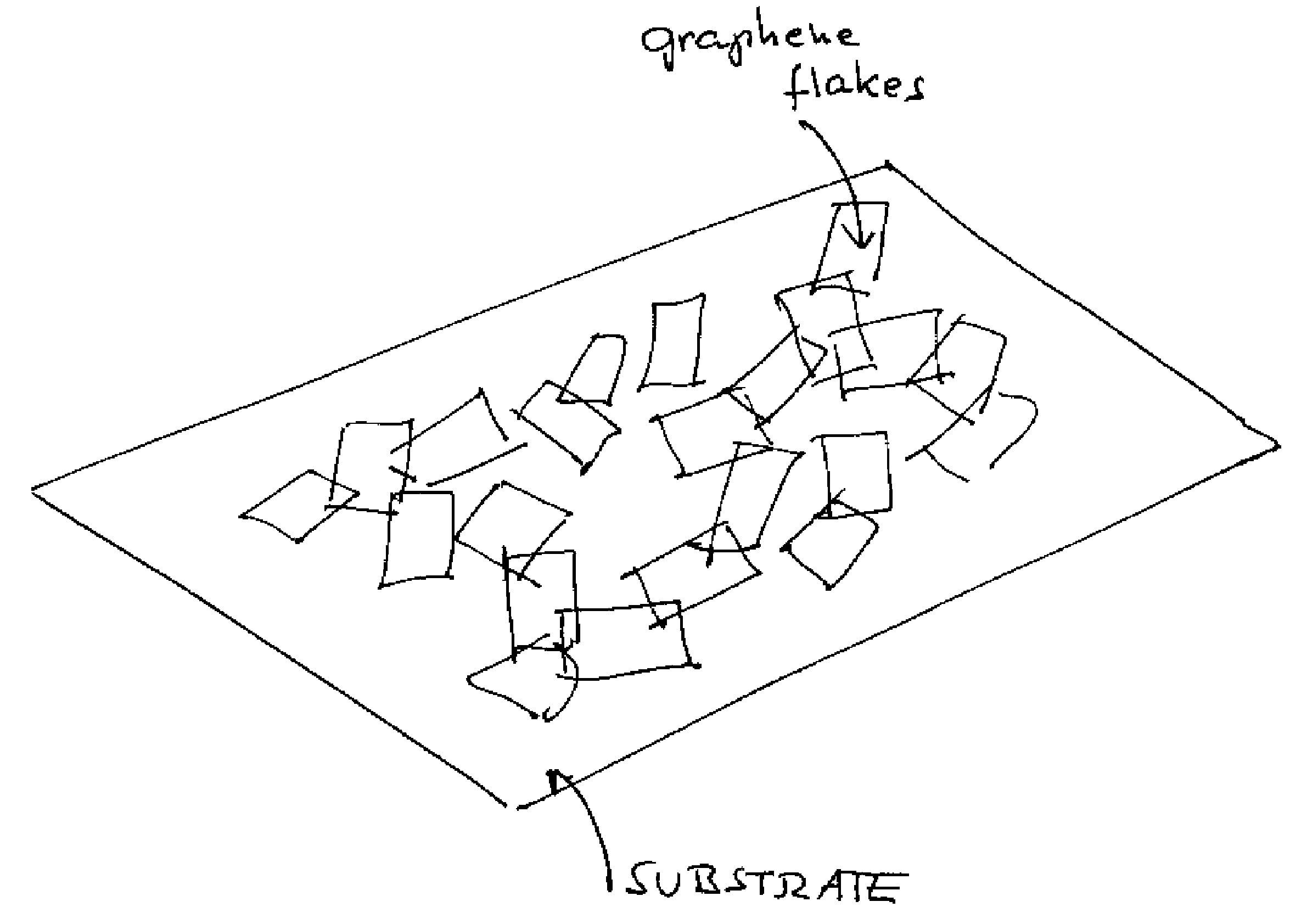
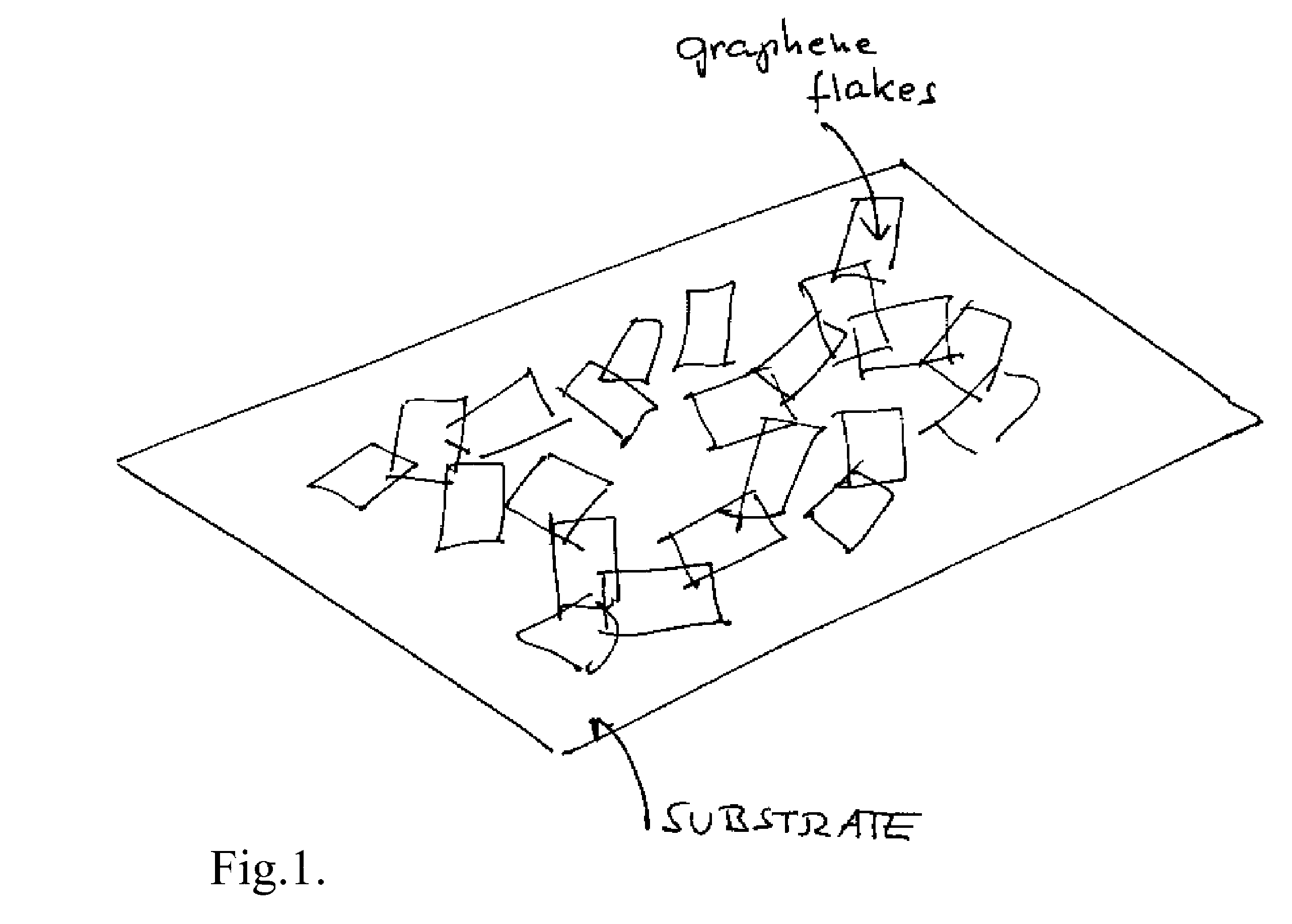
[0019]A first embodiment of the invention is a film formed by an interconnected network of graphene flakes so that there is at least one conduction path across the film.

[0020]Figure one illustrates graphene flakes on a substrate, and figure three provides an SEM image of a graphene flake on a substrate.

[0021]First, commercially available graphene flakes are obtained. The graphene flakes can be treated depending on the desired transparency and conductivity of the resulting films. Examples of preparation steps that can be used to tailor the properties of the resulting films include, but are not limited to, thinning the graphene flakes or doping the graphene flakes. After the graphene flakes have been properly prepared, they are dissolved in solvents such as organic solvents such as dichlorobenzene, chloroform, or dimethylformamide. The solvent can include aqueous dispersions with a suitable surfactant as a solubilization agent. The solvent can also include other solubil...

second embodiment

tworks of Graphene Sheets And Carbon Nanotubes

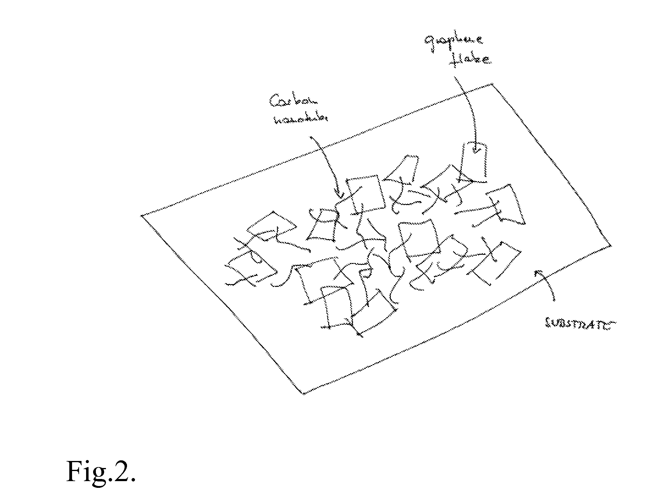
[0025]In another embodiment of the invention, graphene flakes are deposited in combination with other nanostructured materials, in particular carbon nanotubes, so that an interconnected graphene and nanotube layer provides electrical conduction. Figure two is an illustration of a graphene flakecarbon nanotube network, and figure four is an SEM image of a graphene flakecarbon nanotube network.

example

[0026]A graphene flake-carbon nanotube composite was fabricated by repeating the method for the fabrication of the graphene films, with the addition of carbon nanotubes to the solvent. An interpenetrating network of graphene flakes and carbon nanotubes also leads to a network that is 80% transparent and 2 kOhms / sq or 65% and 1 kOhm / sq, where the optical transmission spectra for a 1 kOhm / sq sample is shown in FIG. 5.


PUM

PropertyMeasurementUnit
optical transparencyaaaaaaaaaa
semi-transparentaaaaaaaaaa
dc conductivityaaaaaaaaaa

Abstract

A transparent and conductive film comprising at least one network of graphene flakes is described herein. This film may further comprise an interpenetrating network of other nanostructures, a polymer and / or a functionalization agent(s).

Description

[0001]This application claims priority to U.S. Provisional Patent Application No. 60 / 812,977, filed Jun. 13, 2006, and entitled “GRAPHENE FILM AS TRANSPARENT AND ELECTRICALLY CONDUCTING MATERIAL,” which is hereby incorporated herein by reference.FIELD OF THE INVENTION[0002]The present invention relates generally to transparent and conducting films, and more specifically to transparent and conducting films comprising at least one network of graphene.BACKGROUND OF THE INVENTION[0003]Many modern and / or emerging applications require at least one device electrode that has not only high electrical conductivity, but high optical transparency as well. Such applications include, but are not limited to, touch screens (e.g., analog, resistive, improved analog, X / Y matrix, capacitive), flexible displays (e.g., electro-phoretics, electro-luminescence, electrochromatic), rigid displays (e.g., liquid crystal (LCD), plasma (PDP), organic light emitting diode (LED)), solar cells (e.g., silicon (amor...

Claims


Application Information

Patent Timeline
Patent Type & Authority Patents(United States)
IPC IPC(8): H01B1/24H01B1/00H01B1/04H01B1/20
CPCB82Y30/00B82Y40/00C01B31/0484H01B1/24C01B2204/04Y10S977/737Y10S977/734Y10S977/834Y10S977/832Y10S977/753Y10S977/742C01B32/194
Inventor GRUNER, GEORGEHU, LIANGBINGHECHT, DAVID
Owner SAMSUNG ELECTRONICS CO LTD
Learn More