Semiconductor nano-wire devices and methods of fabrication

a technology of semiconductor nano-wires and nano-wires, which is applied in the direction of semiconductor devices, electrical equipment, nanotechnology, etc., can solve the problems of parasitic off-state leakage, difficult to meet body-doping concentration requirements, gate oxide thickness, etc., and achieve the effect of reducing the likelihood of nano-wire necking or breaking, or possibly eliminating the likelihood of agglomeration of silicon atoms in or near the source and drain region

Inactive Publication Date: 2008-11-18
TAIWAN SEMICON MFG CO LTD
View PDF84 Cites 101 Cited by
  • Summary
  • Abstract
  • Description
  • Claims
  • Application Information

AI Technical Summary

Benefits of technology

[0010]An advantageous feature of the present invention is that the likelihood of necking (narrowing down) or breaking of the nano-wire is reduced or possibly eliminated. Another advantageous feature of the present invention is that the agglomeration of silicon atoms in or near the source and drain regions is substantially reduced.

Problems solved by technology

Hence, a transistor with a short gate length often suffers from problems related to the inability of the gate to substantially control the on / off states of the channel.
However, for device scaling well into the sub-20 nm regime, the requirements for body-doping concentration, gate oxide thickness, and source / drain doping profiles become increasingly difficult to meet using conventional device structures based on bulk silicon substrates.
This may result in a parasitic off-state leakage.
However, this method requires a large amount of oxidation, and hence a large amount of oxide formation, to convert the rectangular channel cross-section shape to a rounded or circular channel cross-section.

Method used


Image

  • Semiconductor nano-wire devices and methods of fabrication
  • Semiconductor nano-wire devices and methods of fabrication
  • Semiconductor nano-wire devices and methods of fabrication

Examples


Embodiment Construction

[0020]The use of presently preferred embodiments is discussed in detail below. It should be appreciated, however, that the present invention provides many applicable inventive concepts that can be embodied in a wide variety of specific contexts. The specific embodiments discussed are merely illustrative of specific ways to make and use the invention, and do not limit the scope of the invention.

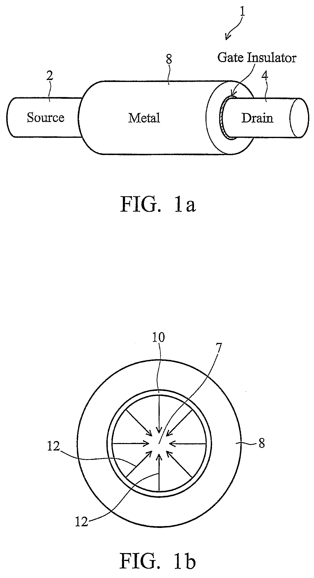
[0021]Example embodiments of the present invention will be described herein in a specific context of making semiconductor devices, such as transistors. In other embodiments not shown, embodiments of the present invention also may include nano-wires or quantum-wires formed in accordance with the present invention. The present invention may also be applied, however, to other situations.

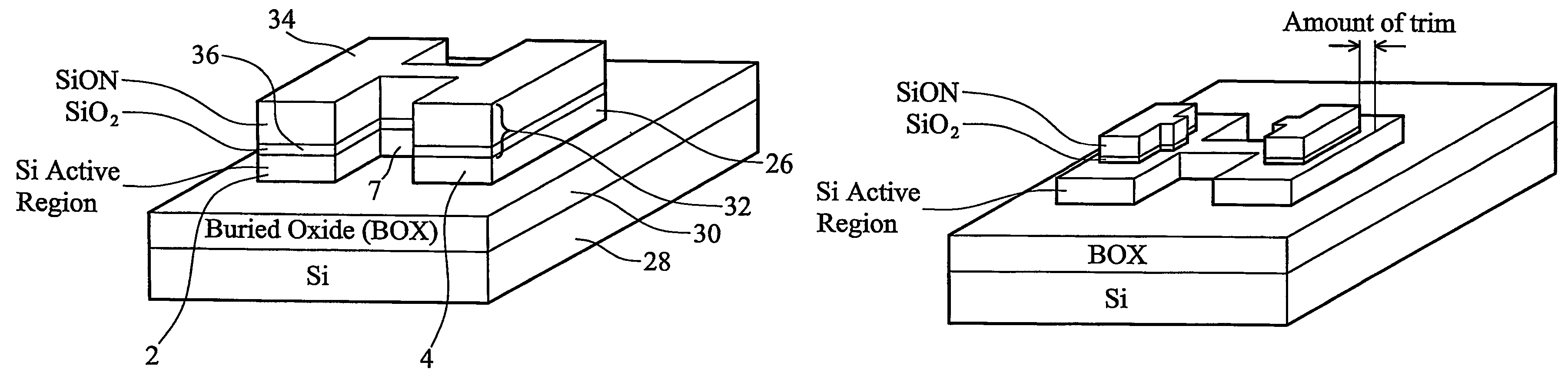
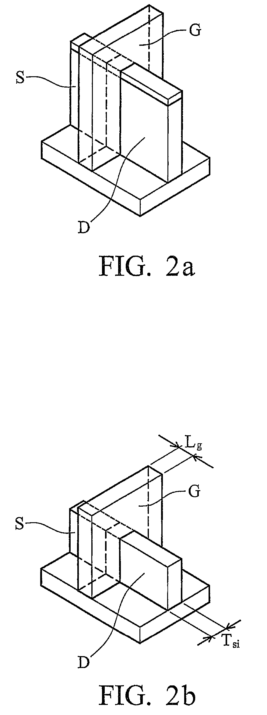
[0022]FIGS. 2a through 2c show the evolution of multiple-gate transistors or FinFETs. FinFETs are essentially field effect transistors with a fin-like or wire-like body region, as illustrated in FIG. 2. The conven...


PUM

PropertyMeasurementUnit
pressureaaaaaaaaaa
pressureaaaaaaaaaa
temperatureaaaaaaaaaa

Abstract

Nano-wires, preferably of less than 20 nm diameter, can be formed with minimized risk of narrowing and breaking that results from silicon atom migration during an annealing process step. This is accomplished by masking portion of the active layer where silicon atomer would otherwise agglomerate with a material such as silicon dioxide, silicon nitride, or other dielectric that eliminates or substantially reduces the silicon atom migration. Nano-wires, nanotubes, nano-rods, and other features can be formed and can optionally be incorporated into devices, such as by use as a channel region in a transistor device.

Description

[0001]This application claims priority to provisional patent application Ser. No. 60 / 578,673 filed on Jun. 10, 2004, entitled “Semiconductor Nanowire Devices and Methods of Fabrication,” which application is hereby incorporated herein by reference.TECHNICAL FIELD[0002]The present invention relates generally to methods for manufacturing semiconductor devices. In particular, this invention teaches a method of forming a nano-wire structure for a channel of a field effect transistor.BACKGROUND[0003]Metal-oxide-semiconductor field effect transistors (MOSFETs) are used in ultra-large scale integrated (ULSI) circuits, which are found in today's semiconductor integrated circuit (IC) chip products. The gate length of the MOSFET is continuously being scaled down for faster circuit speed, higher circuit density and increased functionality, and lower cost per unit function. As the gate length of the MOSFET is scaled into the sub-20 nm regime, the source and drain increasingly interact with the ...

Claims


Application Information

Patent Timeline
Patent Type & Authority Patents(United States)
IPC IPC(8): H01L21/336H01L29/423H01L29/786H01L29/788
CPCB82Y10/00H01L29/0673H01L29/42384H01L29/66795H01L29/7854H01L29/78645H01L21/324H01L29/42392H01L29/78696
Inventor CHEN, HUNG-WEIYEO, YEE-CHIALEE, DI-HONGYANG, FU-LIANGHU, CHENMING
Owner TAIWAN SEMICON MFG CO LTD
Why Eureka
Try Eureka