

Dielectric element, piezoelectric element, ink jet head and ink jet recording apparatus and manufacturing method of same
a piezoelectric element and piezoelectric technology, applied in the direction of device material selection, packaging foodstuffs, packaging goods, etc., can solve the problems of defective characteristics of electronic devices, low electric field intensity applied to a pzt layer, physical destruction of films or on film interfaces, etc., to achieve low-voltage drive and good characteristics
- Summary
- Abstract
- Description
- Claims
- Application Information
AI Technical Summary
Benefits of technology
Problems solved by technology
Method used
Image

Examples
first embodiment
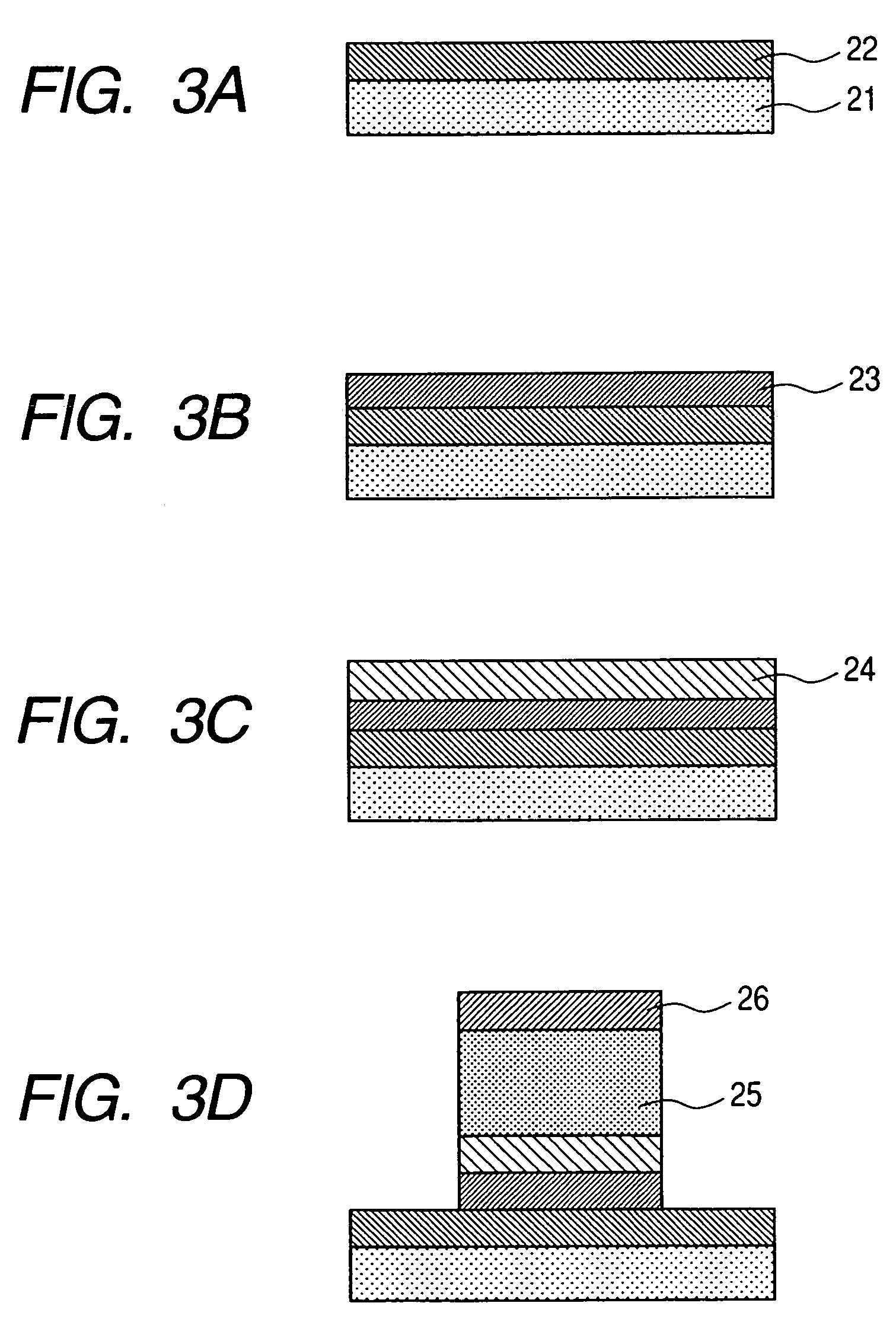
[0096]A Pt (100) orientation film was formed in 120-nm thickness on an MgO (100) substrate, and the first dielectric layer of the present invention was formed thereon in 60-nm thickness at substrate temperature of 590° C. by means of magnetron sputtering by using a target of which composition is Pb (Mg1 / 3Nb2 / 3)O3 and the Pb amount is excessive by 10 percent. This film was a (001) single-orientation film by XRD measurement.
[0097]The second dielectric layer of a PMN-PT layer ([Pb (Mg1 / 3Nb2 / 3)O3]0.67-[PbTiO3]0.33) was film-formed on the PMN layer at substrate temperature of 620° C., and the thin film of 100 nm with a good crystalline orientation was obtained. As for the target in this case, a green compact was used, which was created through heat treatment by mixing a powder of which PbTiO3 component is excessive by 100 percent with a PMN powder. To be more specific, ([Pb (Mg1 / 3Nb2 / 3)O3]0.67-[PbTiO3]0.66) was used as the target composition. The thin film of targeted relative proportion...
sixth embodiments
Second to Sixth Embodiments
[0102]The ink jet head was created in the configuration described in Table 1 by changing the composition of each dielectric layer compared to the first embodiment. In any case, the thin film of a good (001) orientation could be obtained. However, the compositions in Table 1 are composition formulas. As a result of an ICP analysis, Pb is excessive in a range of 1.02 to 1.25, and the characteristics were especially good in that case. The crystalline property of the first layer in a sixth embodiment was 80 percent, and that of the second layer was also 80 percent so that the film of good crystalline property could be obtained.
[0103]
TABLE 1CrystalExampleComposition ofThicknessComposition ofThicknessTarget CompositionOrientationNo.First Layer(μm)ε1Second Layer(μm)ε2of Second Layer(%)2Pb(Zn1 / 3Nb2 / 3)O30.04670[Pb(Zn1 / 3Nb2 / 3)O3]0.91-3.1680[Pb(Zn1 / 3Nb2 / 3)O3]0.91-62[PbTiO3]0.09[PbTiO3]0.183Pb(Sc1 / 2Nb1 / 2)O30.07750[Pb(Sc1 / 2Vb1 / 2)O3]0.55-2.5660[Pb(Sc1 / 2Nb1 / 2)O3]0.55-90[...
seventh embodiment
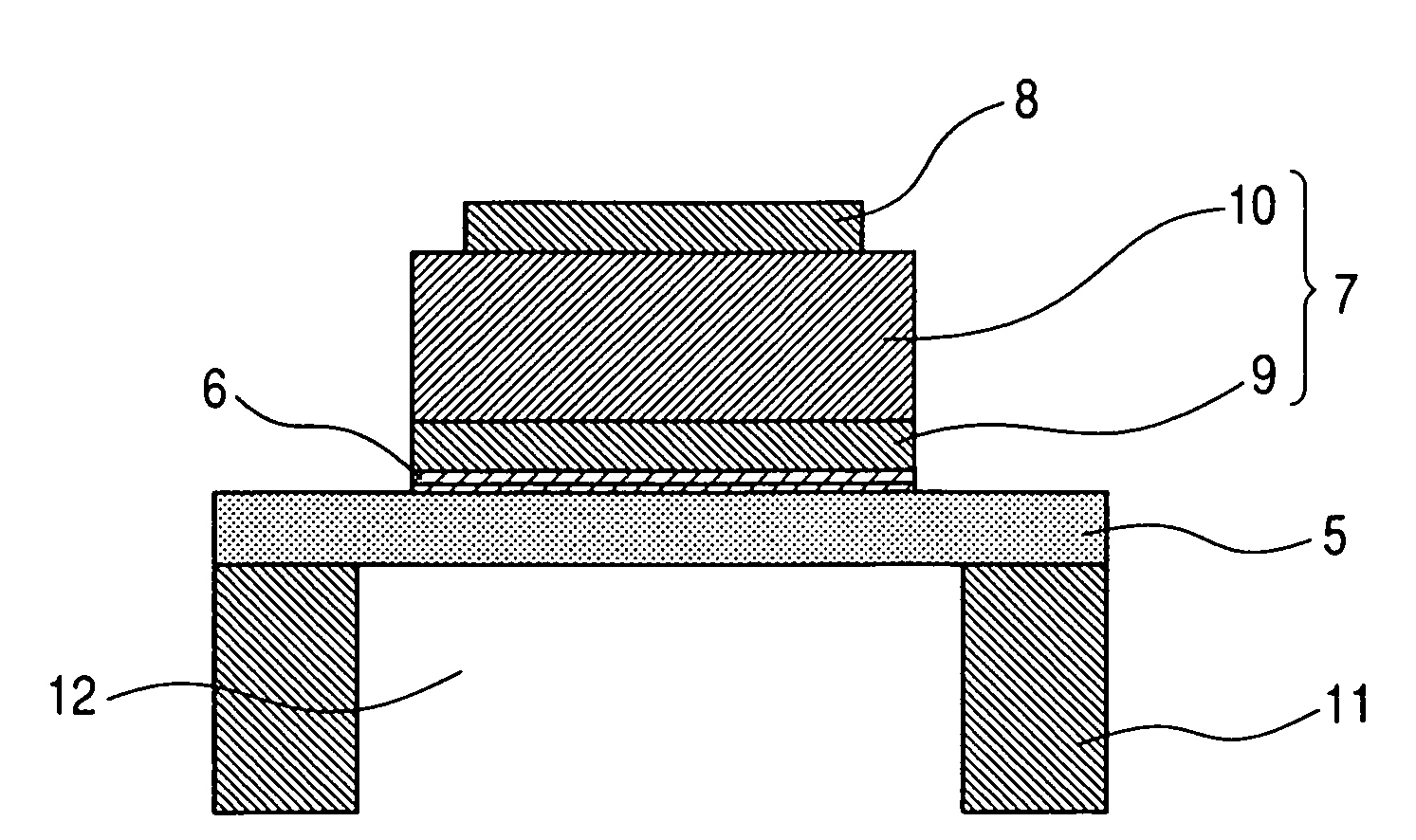
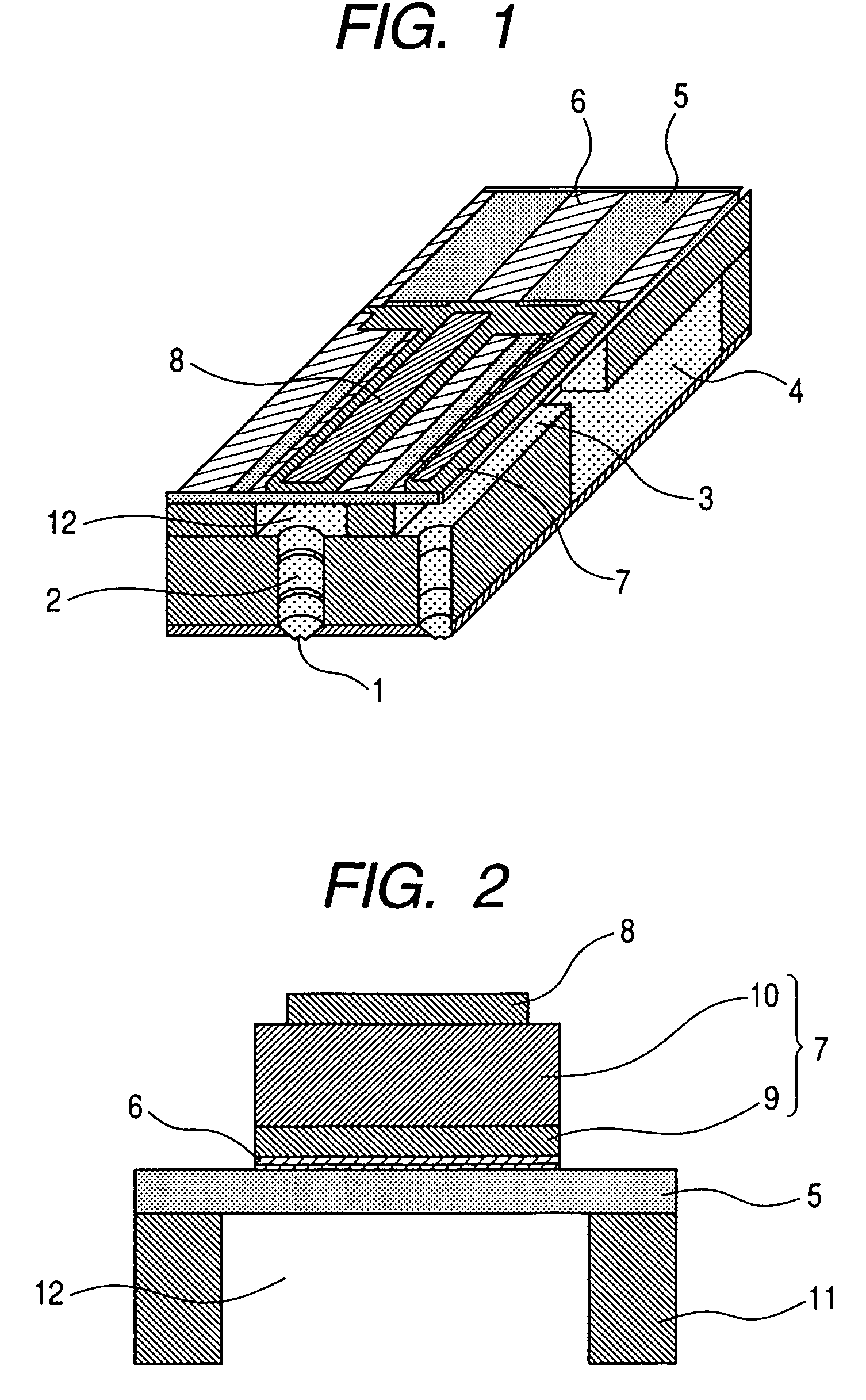
[0104]A YSZ (100) layer was film-formed in 0.1-μm thickness on the SOI layer by using the SOI substrate of which SOI (100) layer is 2 μm thick, SiO2 layer is 0.2 μm thick, handling layer Si (110) is 650 μm thick. An Ir (111) single-orientation film of 0.15 μm was formed thereon, the first layer of Pb (Mg1 / 3Nb2 / 3)O3 was film-formed in 0.1-μm thickness, and the second layer indicated by the composition formula of [Pb (Mg1 / 3Nb2 / 3)O3]0.67-[Pb0.7La0.3TiO3]0.33 was film-formed thereon in 2.5-μm thickness. The first layer was film-formed by using the target of which Pb component was excessive by 15 percent, and the second layer was film-formed by using the target of which composition was [Pb (Mg1 / 3Nb2 / 3)O3]0.67-[Pb0.7La0.3TiO3]0.6 and lead was excessive by 10 percent so as to obtain the piezoelectric layer of which second layer had the crystalline property of 85 percent. As with the first embodiment, it was rendered as the ink jet head by creating the individual liquid chamber thereto. It ...
PUM
| Property | Measurement | Unit |
|---|---|---|
| dielectric constants | aaaaa | aaaaa |
| dielectric constant ε2 | aaaaa | aaaaa |
| dielectric constant | aaaaa | aaaaa |
Abstract
Description
Claims
Application Information