Plasma display panel with improved NIR shielding
a technology of nir shielding and plasma display panel, which is applied in the direction of gas discharge vessel/container, gas-filled discharge tube, solid cathode, etc., can solve the problems of difficult formation of nir shielding film using only nir shielding material, long process time, and high manufacturing cost, so as to facilitate the thinning of plasma display panel, reduce manufacturing process, and save manufacturing cost
- Summary
- Abstract
- Description
- Claims
- Application Information
AI Technical Summary
Benefits of technology
Problems solved by technology
Method used
Image

Examples
first embodiment
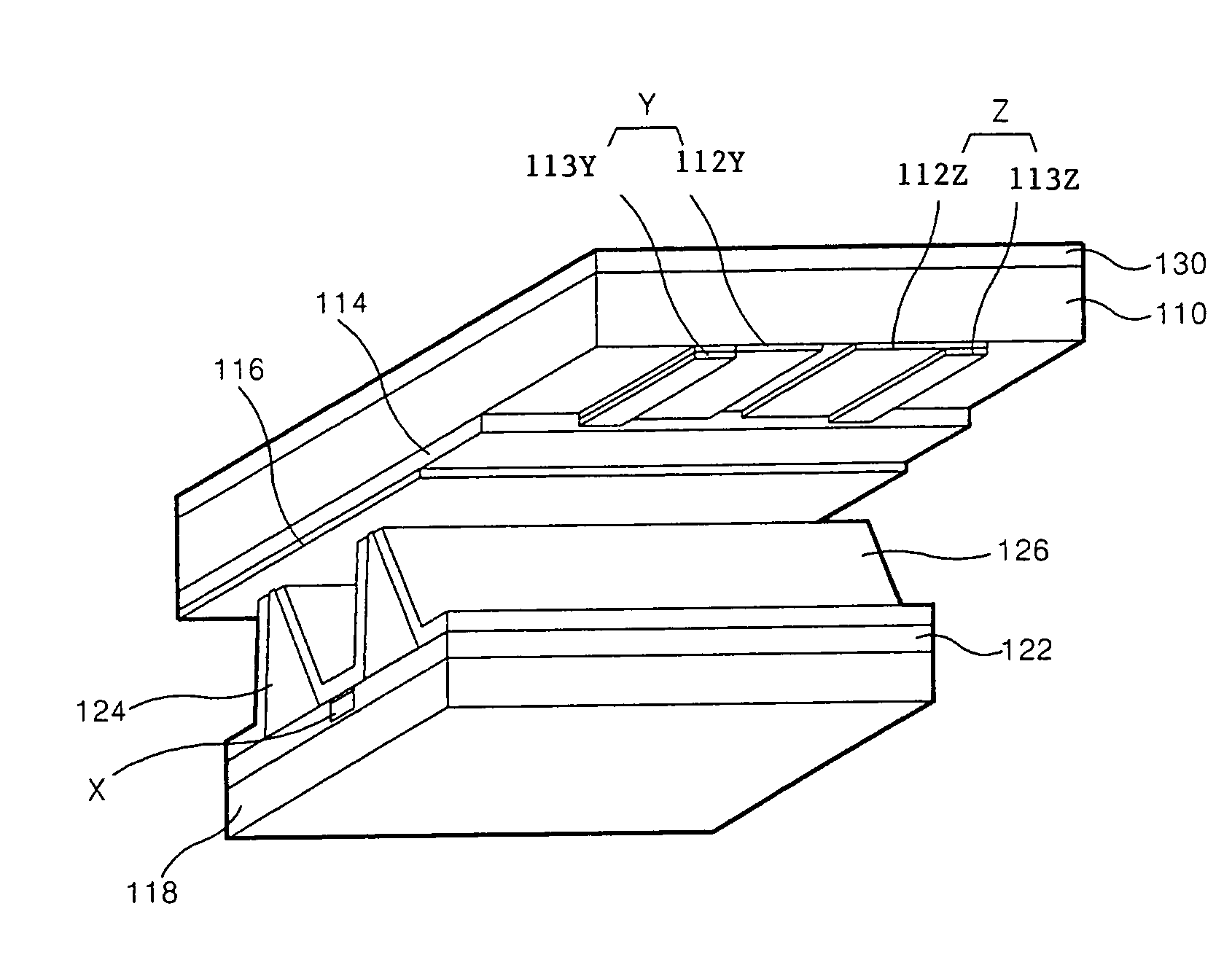
[0054]FIG. 3 illustrates a plasma display panel according to a first embodiment of the present invention.
[0055]Referring to FIG. 3, the plasma display panel according to a first embodiment of the present invention comprises an upper substrate 110 and a lower substrate 118 that are connected with a predetermined distance therebetween.
[0056]Scan electrodes Y and sustain electrodes Z are formed on a bottom surface of the upper substrate 110. The scan electrode Y comprises a transparent electrode 112Y, and a metal bus electrode 113Y, which has a line width smaller than that of the transparent electrode 112Y and is disposed at one side edge of the transparent electrode. Furthermore, the sustain electrode Z comprises a transparent electrode 112Z, and a metal bus electrode 113Z, which has a line width smaller than that of the transparent electrode 112Z and is disposed at one side edge of the transparent electrode.
[0057]The transparent electrodes 112Y, 112Z are generally formed of ITO and a...
second embodiment
[0078]A plasma display panel according to a second embodiment of the present invention comprises an upper substrate and a lower substrate that are connected with a predetermined distance therebetween, in the same manner as the plasma display panel according to the first embodiment of the present invention.
[0079]Scan electrodes and sustain electrodes are formed on a bottom surface of the upper substrate. The scan electrode comprises a transparent electrode, and a metal bus electrode, which has a line width smaller than that of the transparent electrode and is disposed at one side edge of the transparent electrode. Furthermore, the sustain electrode comprises a transparent electrode, and a metal bus electrode, which has a line width smaller than that of the transparent electrode and is disposed at one side edge of the transparent electrode. Furthermore, an upper dielectric layer and a protection layer are laminated on the upper substrate on which the scan electrodes and the sustain el...
third embodiment
[0089]A plasma display panel according to a third embodiment of the present invention comprises an upper substrate and a lower substrate that are connected with a predetermined distance therebetween, in the same manner as the plasma display panel according to the first and second embodiments of the present invention.
[0090]In the third embodiment of the present invention, a NIR shielding material for shielding NIR is comprised in the upper substrate unlike the first and the second embodiment of the present invention. Therefore, the NIR shielding film that has been included in the front filter in the related art can be obviated.
[0091]An address electrode is formed on the lower substrate. A lower dielectric layer and barrier ribs are laminated on the lower substrate on which the address electrode is formed. A phosphor layer is coated on the surfaces of the lower dielectric layer and the barrier ribs. In this case, description on each of the constituent elements other than the protectio...
PUM
 Abstract
Description
Claims
Application Information
 - R&D
- Intellectual Property
- Life Sciences
- Materials
- Tech Scout
- Unparalleled Data Quality
- Higher Quality Content
- 60% Fewer Hallucinations
Browse by: Latest US Patents, China's latest patents, Technical Efficacy Thesaurus, Application Domain, Technology Topic, Popular Technical Reports.
© 2025 PatSnap. All rights reserved.Legal|Privacy policy|Modern Slavery Act Transparency Statement|Sitemap|About US| Contact US: help@patsnap.com