Separate absorption and detection diode for VLWIR

a detection diode and absorption technology, applied in the field of radiation detection, can solve the problems of photodiodes, like other electrical devices, experiencing noise on current signals, not being normally practicable, and making images less understandabl

Active Publication Date: 2008-12-02
DRS NETWORK & IMAGING SYST
View PDF16 Cites 13 Cited by
  • Summary
  • Abstract
  • Description
  • Claims
  • Application Information

AI Technical Summary

Benefits of technology

[0006]Many types of photodiodes operate in reverse bias mode. Diodes typically have high impedance when reverse biased, and light of a proper frequency can generate charge carriers to move from the valence band into the conduction band, and are detected in the high impedance diode circuit, thereby allowing sensitive measurement of the light.
[0025]wide bandgap nature of diode depletion region enables significant reduction in dark current;

Problems solved by technology

Photodiodes, like other electrical devices, experience noise on the current signal.
This is not normally possible in practice.
Dark current not only provides a background “noise” signal which makes images less understandable, but also increases the power consumption of the device.
However, such cooling requirements—especially if cooling much below 0 C is required—add greatly to system cost, bulk, power consumption, and complexity.
Dark current can be particularly problematic for infrared detectors, since the bandgaps of the absorbing material in such detectors are relatively small, in order to permit excitation of carriers into the conduction band by absorbing infrared wavelength photons (which are of relatively low energy).

Method used


Image

  • Separate absorption and detection diode for VLWIR
  • Separate absorption and detection diode for VLWIR
  • Separate absorption and detection diode for VLWIR

Examples


Embodiment Construction

[0045]The numerous innovative teachings of the present application will be described with particular reference to the presently preferred embodiment (by way of example, and not of limitation).

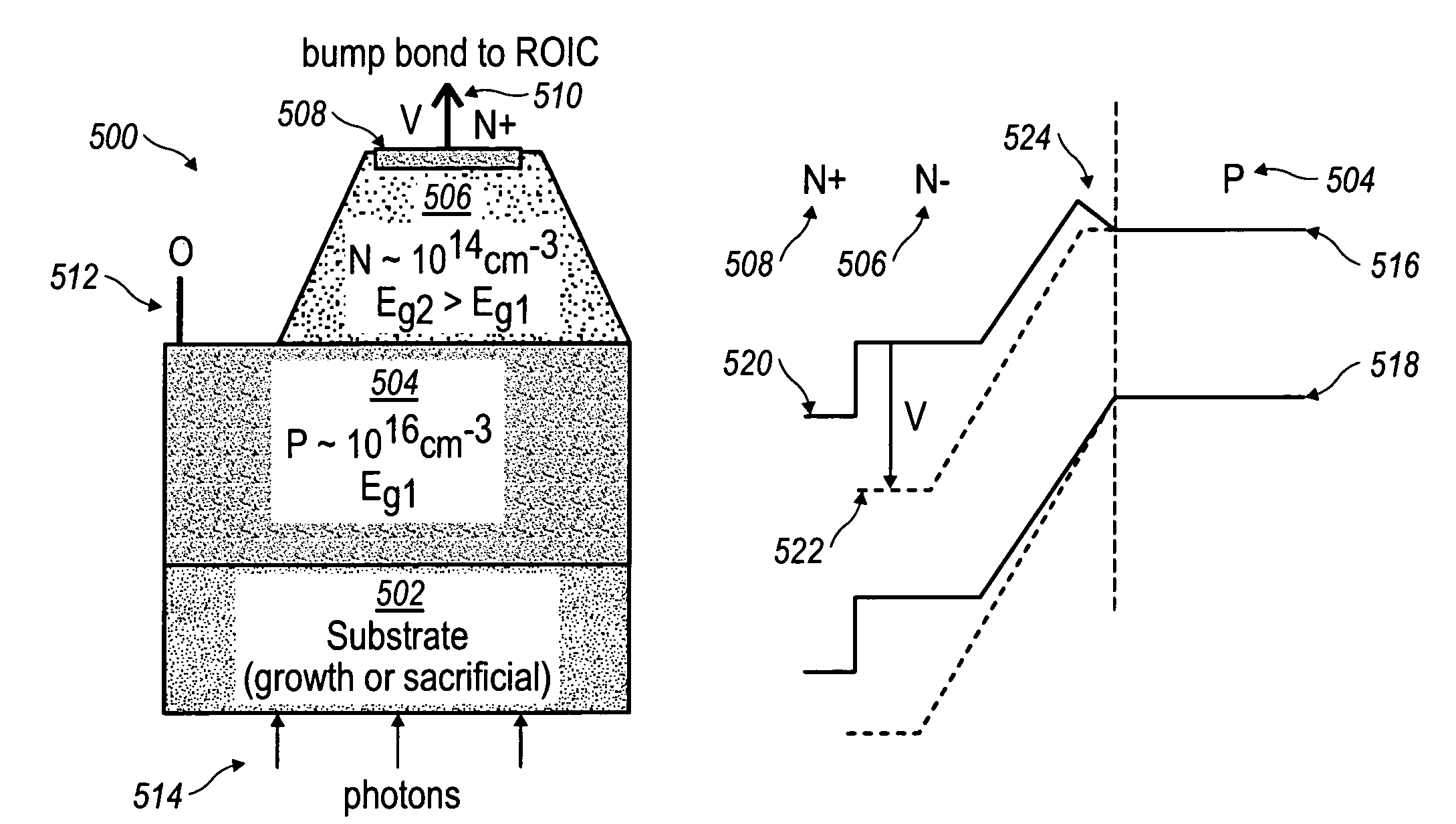
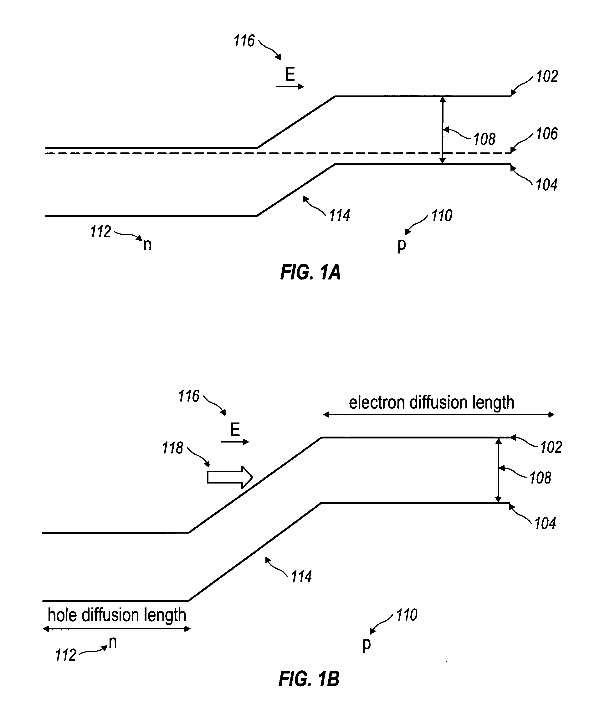
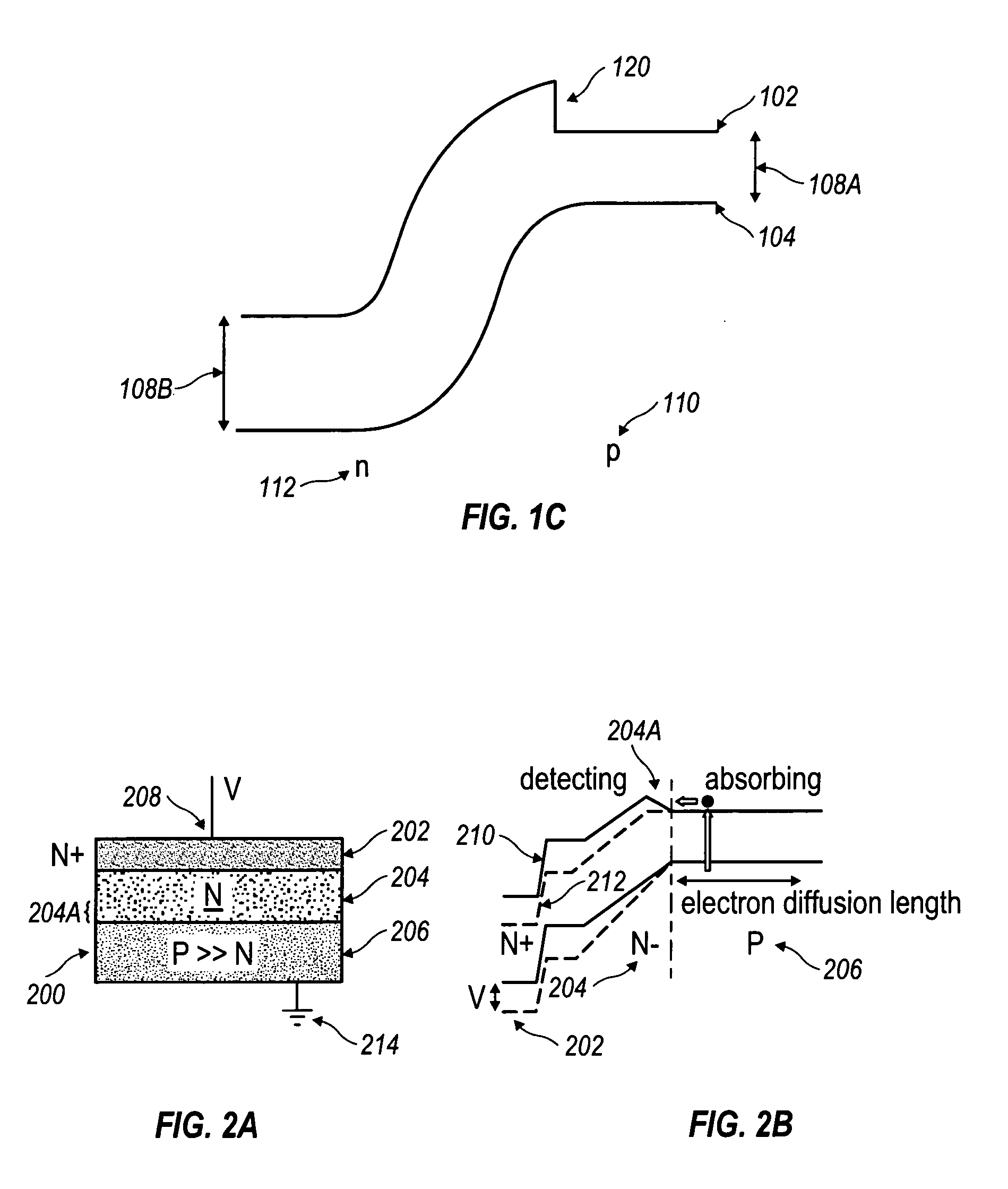
[0046]In one example embodiment, the present innovations include a separate absorption and detection (SAD) diode, having an architecture with a p-type infrared (IR) semiconductor absorbing region coupled to an adjacent n-type region of generally higher bandgap than the absorber region. In preferred embodiments, the p-type region is heavily doped relative to the n-region such that the depletion region of the diode is substantially confined (preferably entirely confined) to the n-type, higher bandgap region of the device. For temperatures such that Nmaj>ni, where ni is the intrinsic carrier concentration of the absorbing p-type region, the overall dark current of a homojunction diode is dominated by generation through S-R centers in the depletion region of the diode. Thus, the wide bandgap nature...


PUM


Abstract

A photodiode for detection of preferably very long wavelength infrared radiation wherein low energy photons are absorbed in one region and detected in another. In one example embodiment, an absorbing P region is abutted with an N region of lower doping such that the depletion region is substantially (preferably completely) confined to the N region. The N region is also chosen with a larger bandgap than the P region, with compositional grading of a region of the N region near the P region. This compositional grading mitigates the barrier between the respective bandgaps. Under reverse bias, the barrier is substantially reduced or disappears, allowing charge carriers to move from the absorbing P region into the N region (and beyond) where they are detected. The N region bandgap is chosen to be large enough that the dark current is limited by thermal generation from the field-free p-type absorbing volume, and also large enough to eliminate tunnel currents in the wide bandgap region of the diode.

Description

CROSS-REFERENCE TO RELATED APPLICATIONS[0001]This application claims priority from U.S. provisional patent application 60 / 718,840 filed on Sep. 20, 2005, which is hereby incorporated by reference.BACKGROUND AND SUMMARY OF THE INVENTION[0002]1. Field of the Invention[0003]The present inventions relate generally to detection of radiation, such as infra-red radiation.[0004]2. Description of Background Art[0005]A photodiode is an electrical component that behaves as a photodetector. Photodiodes are typically implemented as p-n junction diodes that are responsive to optical input, for example, by providing a window, fiber, or other means for photons to impinge on a light-sensitive part of the device.[0006]Many types of photodiodes operate in reverse bias mode. Diodes typically have high impedance when reverse biased, and light of a proper frequency can generate charge carriers to move from the valence band into the conduction band, and are detected in the high impedance diode circuit, th...

Claims


Application Information

Patent Timeline
Patent Type & Authority Patents(United States)
IPC IPC(8): H01L31/072
CPCH01L31/109
Inventor KINCH, MICHAEL A.
Owner DRS NETWORK & IMAGING SYST
Why Eureka
Try Eureka