Apparatus of inspecting defect in semiconductor and method of the same

a technology of defect inspection and inspection apparatus, which is applied in the direction of semiconductor/solid-state device testing/measurement, instruments, material analysis, etc., can solve the problem that the detection accuracy of defect size is now difficult to meet the requirements of inspection apparatus in the related art for various fine patterns including a pattern in a semiconductor device, so as to achieve the effect of improving productivity and accurately calculating the size of a detected d

Active Publication Date: 2009-01-06
HITACHI HIGH-TECH CORP
View PDF15 Cites 27 Cited by
  • Summary
  • Abstract
  • Description
  • Claims
  • Application Information

AI Technical Summary

Benefits of technology

[0010]According to embodiments of the invention, size of a detected defect can be accurately calculated, and for example, only defects having a size larger than a size to be managed can be extracted in semiconductor manufacturing. Thus, since a defect having higher influence on a production yield can be preferentially managed, productivity is improved in semiconductor manufacturing.

Problems solved by technology

As described above, inspection apparatus in the related art for various fine patterns including a pattern in a semiconductor device is now hard to satisfy detection accuracy of defect size required for detection of a defect on an increasingly miniaturized pattern.

Method used


Image

  • Apparatus of inspecting defect in semiconductor and method of the same
  • Apparatus of inspecting defect in semiconductor and method of the same
  • Apparatus of inspecting defect in semiconductor and method of the same

Examples


Embodiment Construction

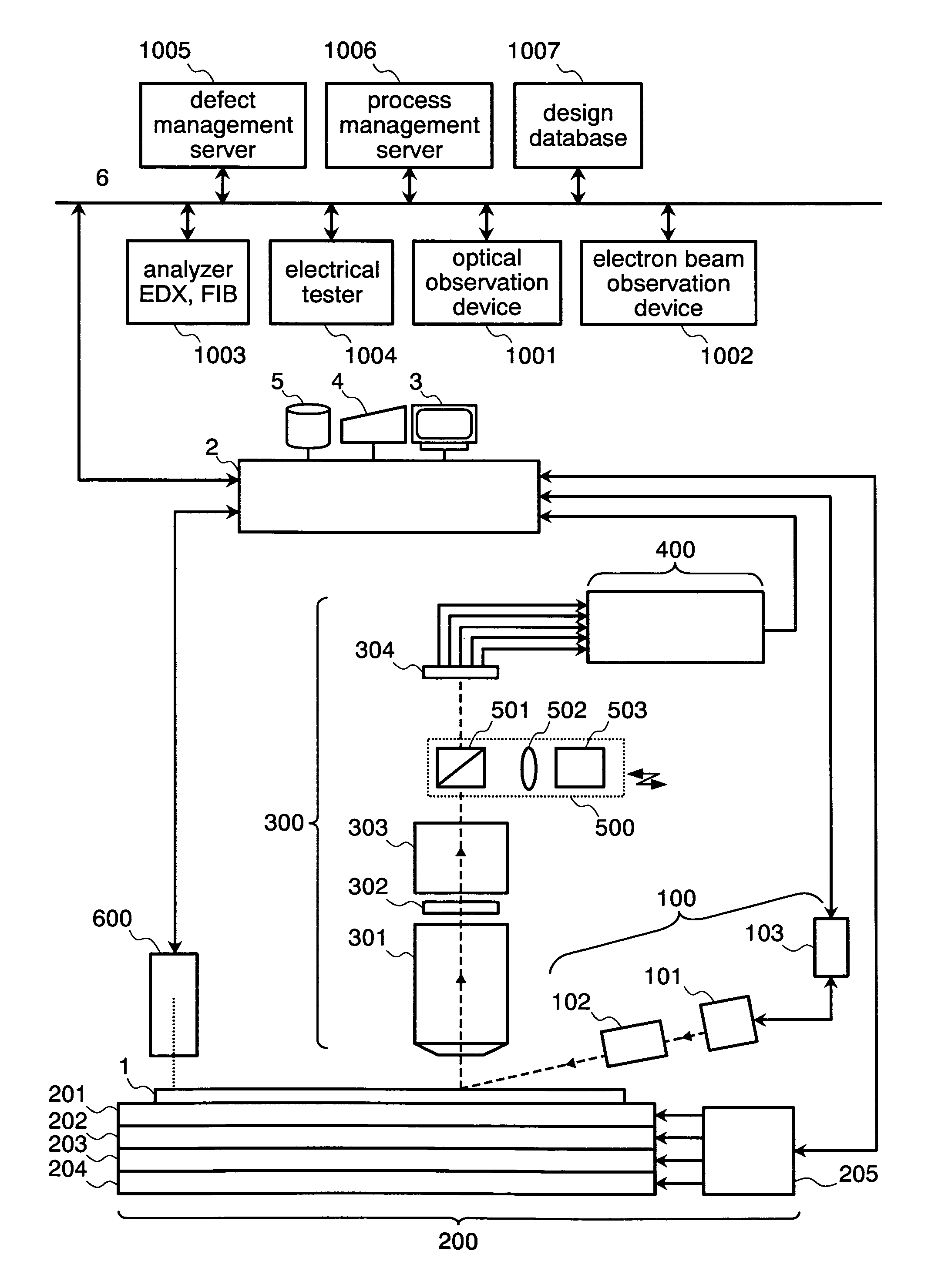
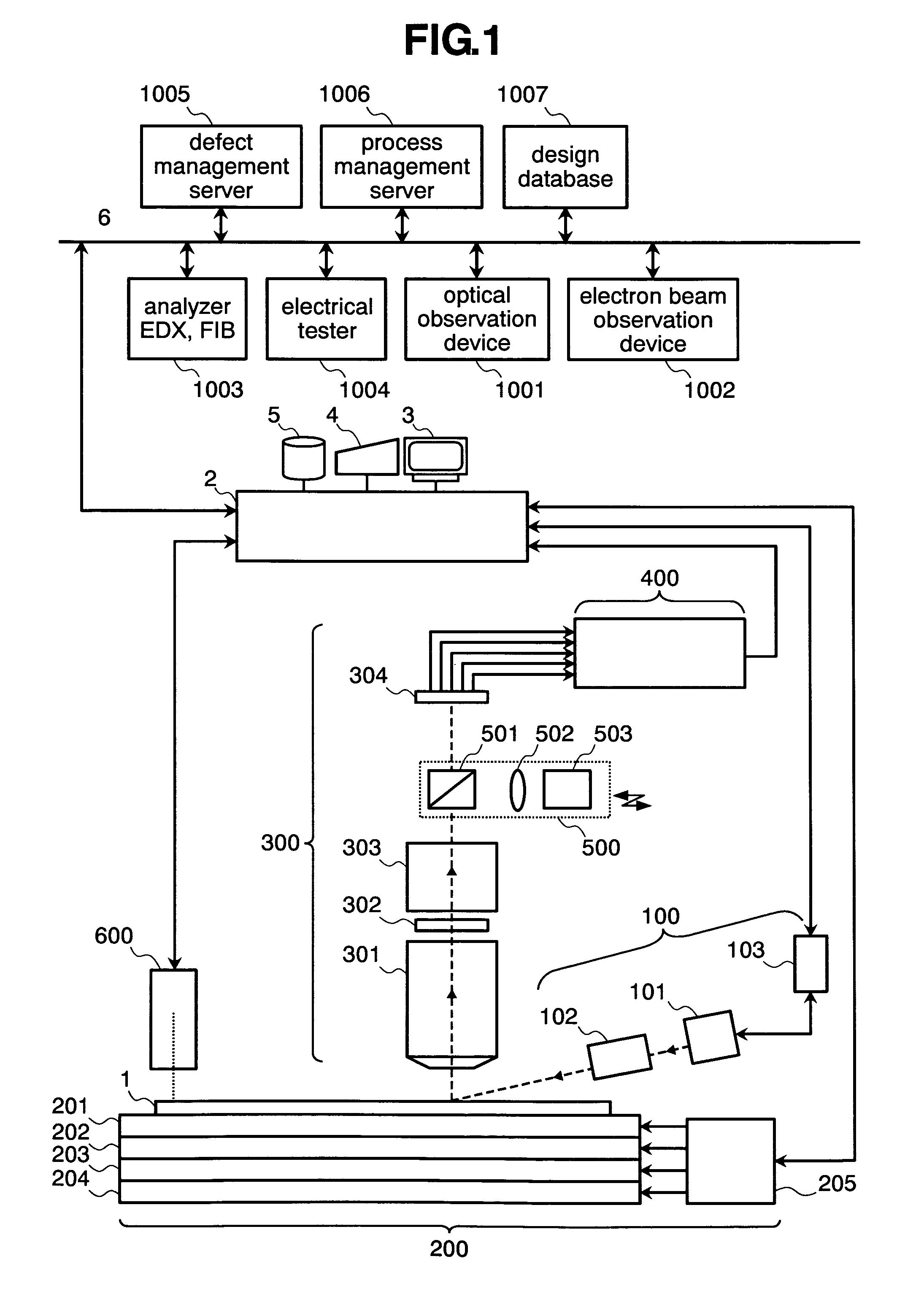
[0029]FIG. 1 shows an example of a configuration of inspection apparatus according to embodiments of the invention (hereinafter, mentioned as defect inspection apparatus).

[0030]The defect inspection apparatus is configured to have an illumination system 100, a stage system 200, a detection system 300, a Fourier transform surface observation system 500, a signal processing section 400, an observation optical system 600, and a control section 2.

[0031]Defect detection using the defect inspection apparatus shown in FIG. 1 is performed according to the following procedure. The illumination system 100 illuminates a wafer 1 set in the stage system 200, and the detection system 300 acquires an image of the illuminated wafer 1. The illumination system 100 adjusts output of a light source 101 by an illumination controller 103 according to an instruction value of the control section 2. As the light source 101, a laser light source is used, which emits laser in an ultraviolet region having a wa...


PUM

PropertyMeasurementUnit
wavelengthaaaaaaaaaa
defect inspectionaaaaaaaaaa
sizeaaaaaaaaaa

Abstract

When size of a defect on an increasingly miniaturized pattern is obtained by defect inspection apparatus in the related art, a value is inconveniently given, which is different from a measured value of the same defect by SEM. Thus, a dimension value of a defect detected by defect inspection apparatus needs to be accurately calculated to be approximated to a value measured by SEM. To this end, size of the defect detected by the defect inspection apparatus is corrected depending on feature quantity or type of the defect, thereby defect size can be accurately calculated.

Description

BACKGROUND OF THE INVENTION[0001]The present invention relates to defect inspection apparatus and a defect inspection method which are used in a manufacturing line of a semiconductor device, liquid crystal device, magnetic head or the like, and particularly relates to a calculation technique of size of a detected defect.[0002]Inspection of a semiconductor wafer is described as an example.[0003]In a semiconductor manufacturing process in the related art, foreign substances on a semiconductor substrate (wafer) may cause inferiority such as imperfect insulation or a short circuit. When a fine foreign substance exists in a semiconductor substrate of a semiconductor element which is significantly miniaturized, the foreign substance may cause imperfect insulation of a capacitor or breakdown of a gate oxide film. The foreign substances may be contaminated in various ways due to various reasons, such as contamination from a movable portion of a carrier device, contamination from a human bod...

Claims


Application Information

Patent Timeline
Patent Type & Authority Patents(United States)
IPC IPC(8): G01N21/88G01B11/00G01B11/02G01N21/956H01L21/66
CPCG01N21/956
Inventor HAMAMATSU, AKIRAMAEDA, SHUNJISHIBUYA, HISAE
Owner HITACHI HIGH-TECH CORP
Why Eureka
Try Eureka