

Method of fabricating photo mask
a technology of photo mask and mask body, which is applied in the direction of photomechanical equipment, instruments, originals for photomechanical treatment, etc., can solve the problems of affecting affecting the lithography technique, and not correcting the layout, so as to increase the accuracy of opc process and improve the productivity of opc process
- Summary
- Abstract
- Description
- Claims
- Application Information
AI Technical Summary
Benefits of technology
Problems solved by technology
Method used
Image

Examples
Embodiment Construction
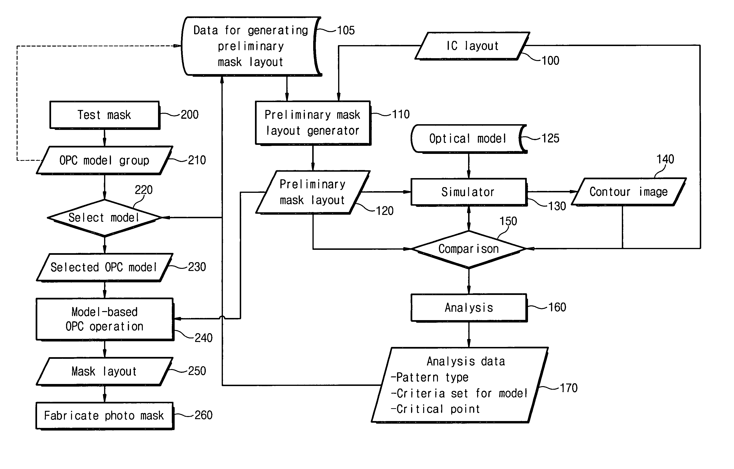
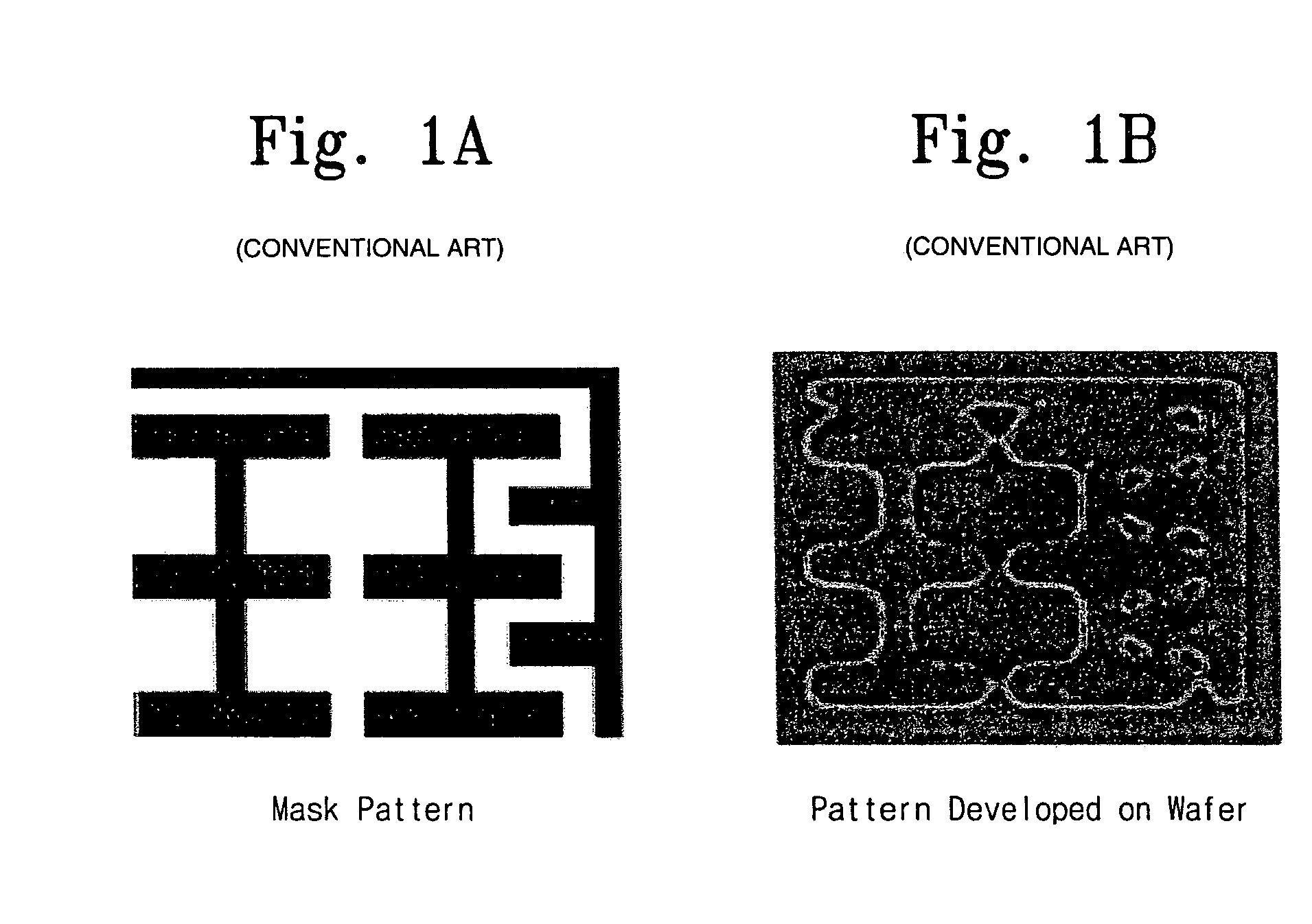
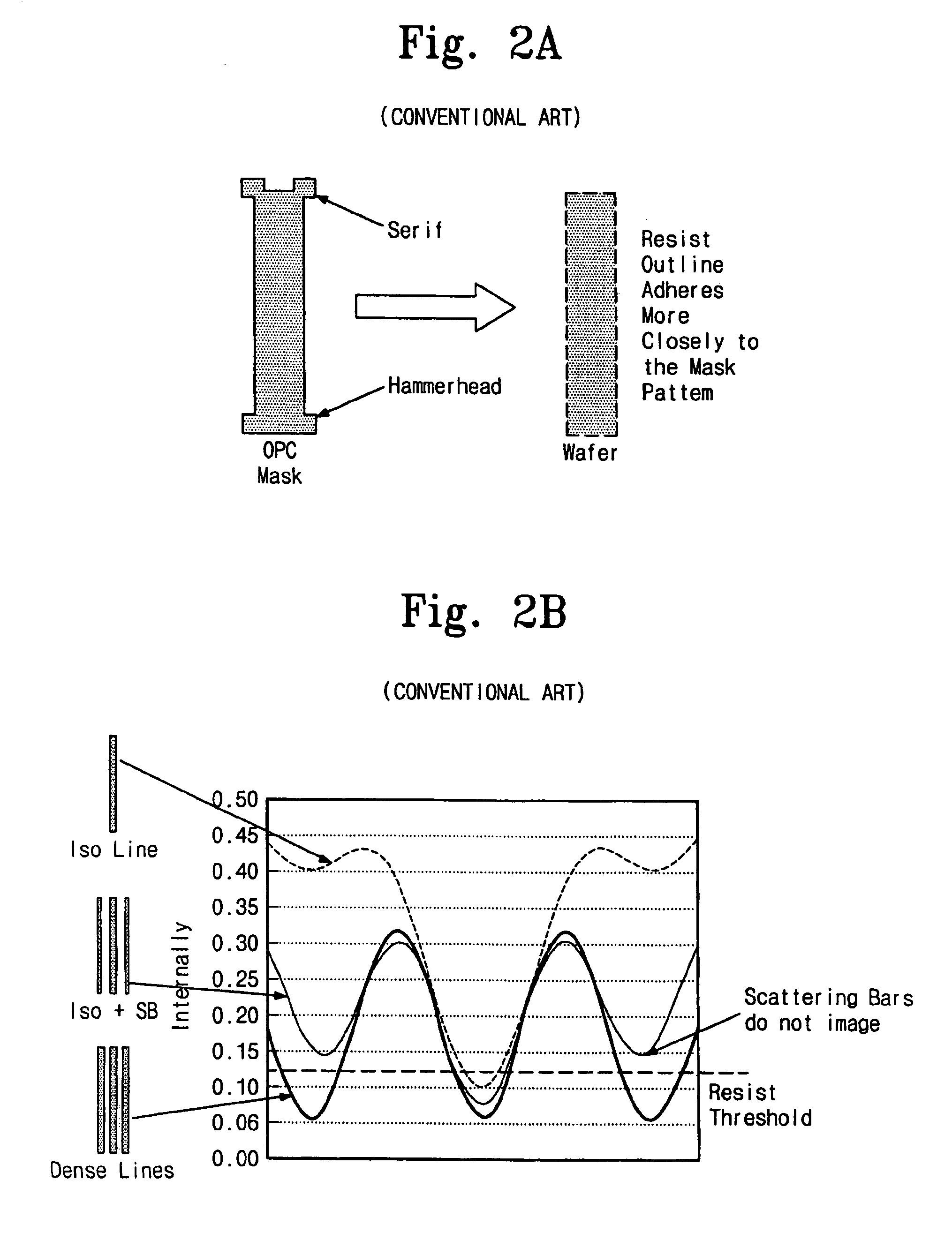
[0043]Reference will now be made in detail to example embodiments, examples of which are illustrated in the accompanying drawings. However, example embodiments are not limited to the embodiments illustrated hereinafter, and the embodiments herein are rather introduced to provide easy and complete understanding of the scope and spirit of example embodiments. In the drawings, the thicknesses of layers and regions are exaggerated for clarity.
[0044]It will be understood that when an element or layer is referred to as being “on,”“connected to” or “coupled to” another element or layer, it may be directly on, connected or coupled to the other element or layer or intervening elements or layers may be present. In contrast, when an element is referred to as being “directly on,”“directly connected to” or “directly coupled to” another element or layer, there are no intervening elements or layers Like reference numerals refer to like elements throughout. As used herein, the term “and / or” include...
PUM
| Property | Measurement | Unit |
|---|---|---|
| optical model | aaaaa | aaaaa |
| critical points | aaaaa | aaaaa |
| dimension | aaaaa | aaaaa |
Abstract
Description
Claims
Application Information