Mask blank for charged particle beam exposure, method of forming mask blank and mask for charged particle beam exposure

a technology for charged particle beams and masks, which is applied in the direction of originals for photomechanical treatment, instruments, transportation and packaging, etc., can solve the problems of large shift in the position of desired patterns such as lsi, difficulty in forming thin silicon layers without defects, and difficulty in uniform thickness, etc., to achieve high reliability in quality

Inactive Publication Date: 2009-01-20
DAI NIPPON PRINTING CO LTD
View PDF41 Cites 6 Cited by
  • Summary
  • Abstract
  • Description
  • Claims
  • Application Information

AI Technical Summary

Benefits of technology

[0017]The present invention is made in order to solve the above described problems. It is an object of the present invention to provide a mask blank used for the charged particle beam exposure made by employing an SOI substrate with a silicon membrane having high reliability in quality, in which however there is no problem of deformation due to the compression stress of a silicon oxide film, as an intermediate layer of the SOI substrate, and to provide a method of forming such a mask blank and a mask used for the charged particle beam exposure.
[0018]In order to achieve the above described object, a mask blank used for the charged particle beam exposure according to the first aspect of the present invention is a mask blank which is made by employing an SOI substrate having a front-side silicon membrane and a back-side silicon layer with a silicon oxide film interposed therebetween, wherein the back-side silicon layer is partially removed to form an opening to be an exposed region of said SOI substrate, the silicon oxide film in the opening is removed, and an etching stop layer having lower stress is formed in the opening.
[0027]According to a method of forming a mask blank and a mask for the charged particle beam exposure of the present invention as mentioned above, after etching the silicon to the silicon oxide film as the intermediate layer by work on the back side of the SOI substrate, the silicon oxide film having higher stress existing in the opening is removed and, instead of the removed silicon oxide film, an etching stop layer having lower internal stress is freshly formed. With this structure, a blank made by employing an SOI substrate having higher reliability in quality concerning zero defects and thickness uniformity, in which however there is no problem of deformation of a silicon membrane can be obtained. By using this blank, the shift of position of pattern due to the internal stress of the etching stop layer can be reduced so that a mask used for charged particle beam exposure can be obtained which has excellent quality and has a pattern of high accuracy of position.

Problems solved by technology

As the mask is formed using the blank 58 with this distortion, a problem is caused that the position of the desired pattern such as LSI may be greatly shifted.
If abnormal particles of silicon are generated, defects are produced.
Accordingly, it is difficult to form a thin silicon layer without defects and having uniform thickness.
Thus, there is a problem that it is hard to obtain a high quality mask using a mask blank prepared by this forming method.

Method used


Image

  • Mask blank for charged particle beam exposure, method of forming mask blank and mask for charged particle beam exposure
  • Mask blank for charged particle beam exposure, method of forming mask blank and mask for charged particle beam exposure
  • Mask blank for charged particle beam exposure, method of forming mask blank and mask for charged particle beam exposure

Examples


Embodiment Construction

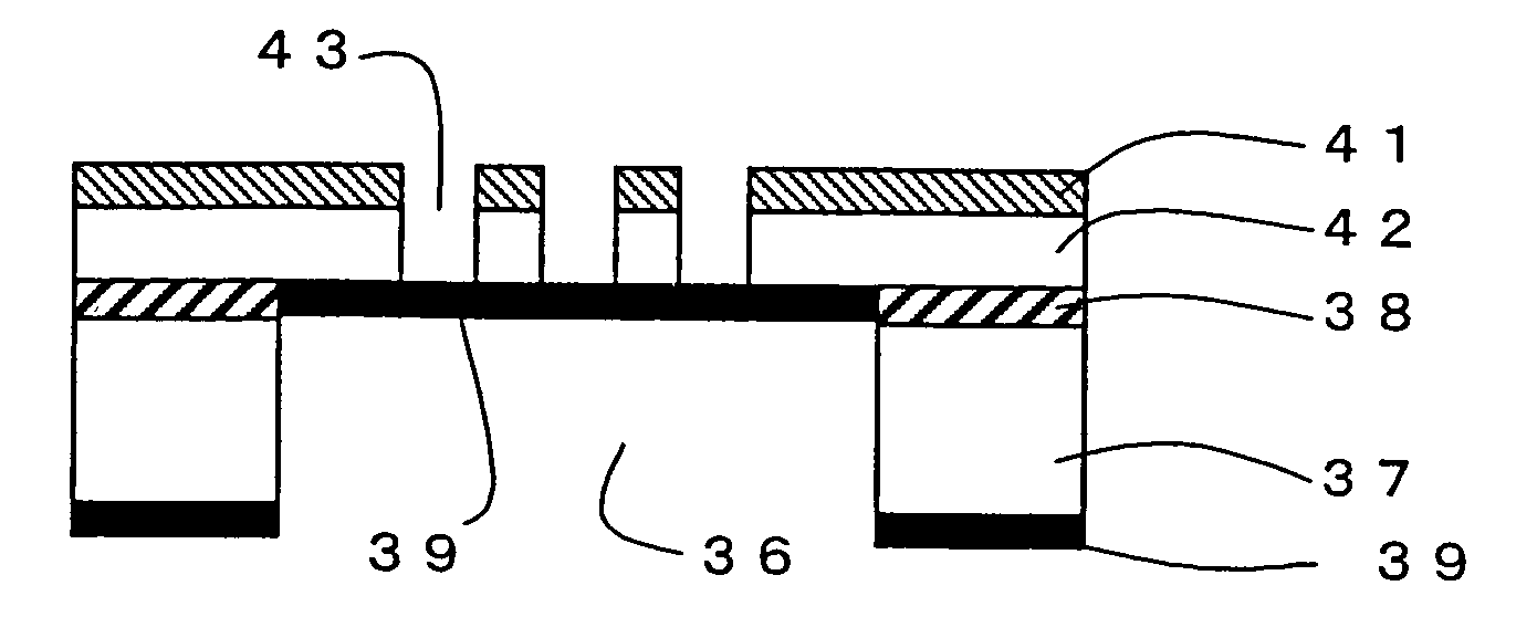
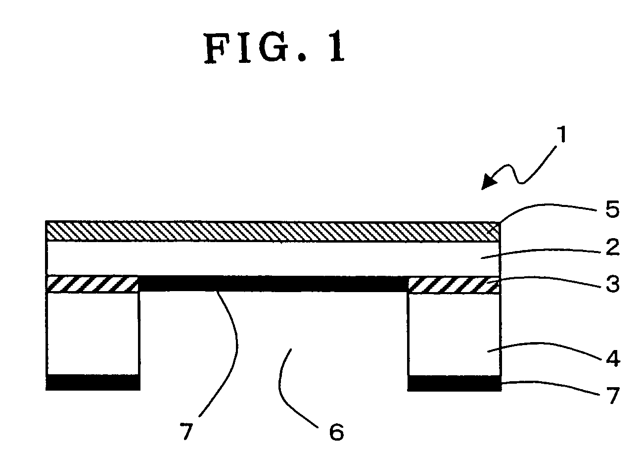
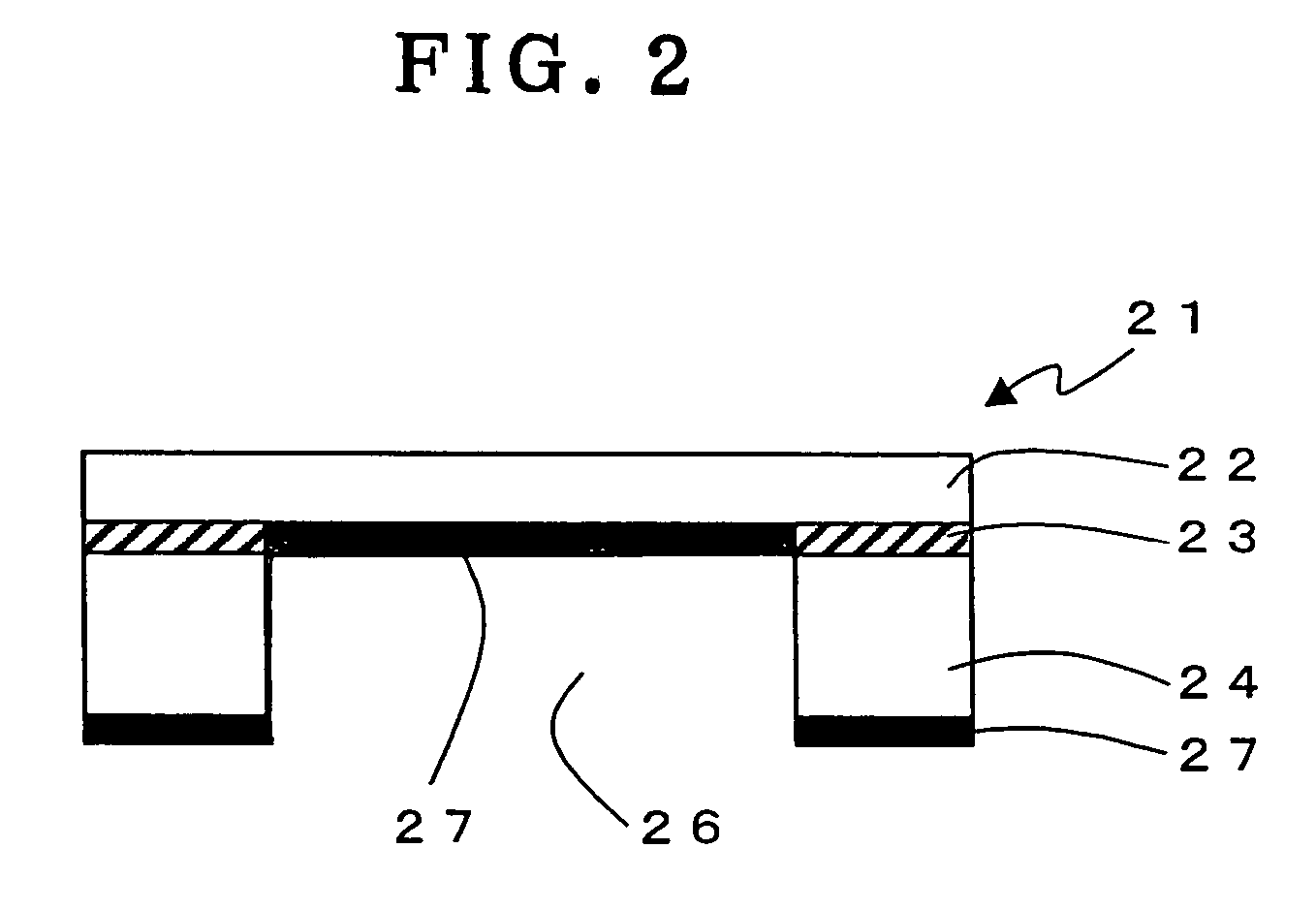
[0036]Hereinafter, embodiments of the present invention will be described, taking electron-beam exposure which is most likely expected to be in practical use among charged particle beam exposure technologies for example. Description will now be made as regard to a mask blank used for the electron-beam exposure and its forming method, and a method of forming a mask used for the electron-beam exposure with reference to the attached drawings.

(Mask Blank Used for the Charged Particle Beam Exposure)

[0037]FIG. 1 is a partial vertical sectional view schematically showing an embodiment of a mask blank used for the electron beam exposure according to the present invention which is used for a stencil mask used for an electron-beam projection lithography. In FIG. 1, a mask blank 1 used for the electron-beam exposure has a structure comprising struts (supporting silicon layer) 4 made of silicon, a silicon membrane 2 which is bonded to the supporting silicon layer 4 with a silicon oxide film 3 i...


PUM

PropertyMeasurementUnit
thicknessaaaaaaaaaa
thicknessaaaaaaaaaa
thicknessaaaaaaaaaa

Abstract

The present invention provides a mask blank used for the charged particle beam exposure made by employing an SOI substrate having a silicon membrane higher reliability in quality, without the problem of deformation due to the compression stress of a silicon oxide film as an intermediate layer of the SOI substrate, and provides a method for forming a mask blank and a mask used for the charged particle beam exposure. The mask blank used for the charged particle beam exposure made by employing an SOI substrate having a front-side silicon membrane and a back-side silicon layer with a silicon oxide layer interposed therebetween is characterized in that the back-side silicon layer and the silicon oxide film of said SOI substrate are partially removed to form an opening to be an exposed region and an etching stop layer having lower stress is formed in the opening.

Description

BACKGROUND OF THE INVENTION[0001]The present invention relates to a method of forming a mask blank and a mask used for the lithography for manufacturing semiconductor devices and, more particularly, to a structure of a mask blank for fabricating a mask which transcribes a mask pattern onto a wafer using charged particle beams such as electron beams and ion beams and a method for forming a mask blank and a mask used for the charged particle beam exposure.[0002]With miniaturization and increase in integration of semiconductor elements in semiconductor integrated circuits, an electron-beam projection lithography for transcribing a predetermined configuration onto a wafer using charged particle beams, especially using electron beams, was developed instead of the conventional photolithography using light. Recently, the development of EPL (Electron-beam Projection Lithography) method achieving higher throughput has advanced. As an electron-beam projection lithography, there is a method in...

Claims


Application Information

Patent Timeline
Patent Type & Authority Patents(United States)
IPC IPC(8): B44C1/22C23F1/00G03F1/20H01L21/027
CPCG03F1/20Y10T428/24851Y10T428/24174H01J2237/31794
Inventor MORIMOTO, KENICHI
Owner DAI NIPPON PRINTING CO LTD
Why Eureka
Try Eureka