

Microcoaxial probes made from strained semiconductor bilayers
a semiconductor bilayer and microcoaxial probe technology, applied in the direction of mechanical measurement arrangement, mechanical roughness/irregularity measurement, instruments, etc., can solve the problem of limited range of scanning microscopy probe frequency available for present scanning probes
- Summary
- Abstract
- Description
- Claims
- Application Information
AI Technical Summary
Benefits of technology
Problems solved by technology
Method used
Image

Examples
example 1
Fabrication of a Microtube from an Si / SiGe Semiconductor Heterostructure
[0032]A bilayer film was grown by deposition of Si onto an SiGe strained layer on insulator (SGOI) using solid-source molecular-beam epitaxy (MBE). The MBE SiGe film had a concentration of ˜20% Ge. For the MBE film, the thickness of Si layer was controlled by rotating a shutter in the MBE chamber. The growth rate was 0.55 Å s−1 at a substrate temperature of 585° C., measured by an optical pyrometer. The MBE growth of the Si layer was monitored by reflection high-energy electron diffraction during the entire growth process.
[0033]The SGOI substrate was obtained from SOITEC (France). The thickness and composition of SGOI were about 44 nm Si with 20% Ge on 190 nm SiO2. The sample was cleaned with 10% hydrofluoric acid to remove the native oxide grown in air on the original SGOI surface, followed by 10 min of cleaning with piranha (H2SO4 / H2O2), and a few seconds 10% HF etching to remove the oxide layer produced durin...
example 2
Fabrication of a Microtube from an Si / SiGe Semiconductor Heterostructure
[0036]Arrays of squares were patterned on SiGe / Si bilayer material (obtained from SOITEC (France)) using electron-beam lithography, aluminium deposition, and lift-off. Reactive-ion etching was used to isolate the bilayer squares from each other. Each array contained 400 squares with identical dimensions. As schematically shown in FIG. 4(a), the bilayer includes a 50-nm-thick layer of relaxed Si0.8Ge0.2 over a 20-nm-thick layer of strained silicon. The 184-nm-thick SiO2 layer served as a sacrificial layer. This heterostructure was realized using the Smart Cut technology, in which the strained silicon layer was initially grown on relaxed Si0.8Ge0.2 and then both layers were transferred to a SiO2 sacrificial layer on the Si substrate. Both planes of the bilayer and substrate were oriented along crystalline direction (001). Squares were patterned so that the edges were parallel to the (110) (±5°) direction and the d...
example 3
Fabrication of a Microtube from an InGaAs / GaAs Semiconductor Heterostructure
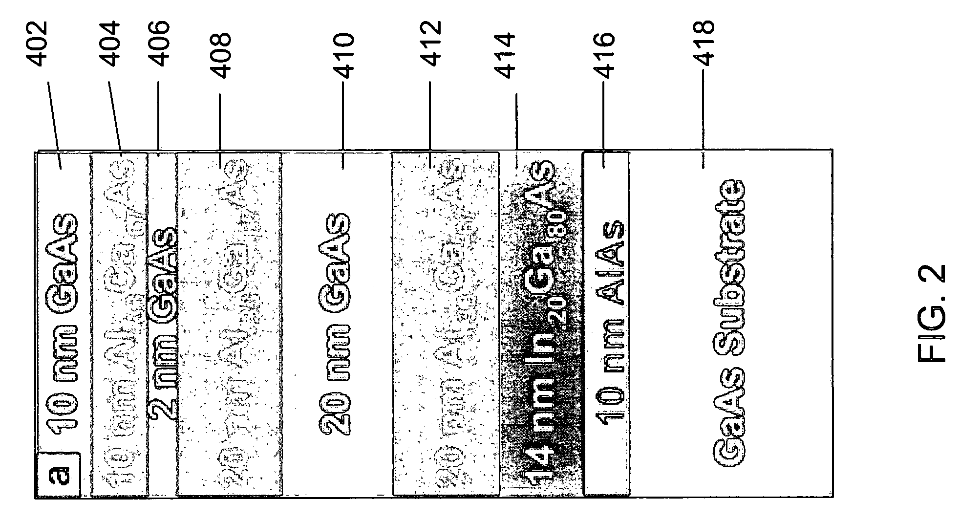
[0038]A heterostructure comprising a transport layer formed by 10 nm GaAs cap layer, followed by 10 nm Al0.33Ga0.67As layer, 2 nm GaAs (Si delta doped) layer, 20 nm Al0.33Ga0.67As layer, 20 nm GaAs layer over the strained bilayers of 20 nm Al0.33Ga0.67As, 14 nm In0.2Ga0.8As and 10 nm AlAs (sacrificial layer) over a GaAs substrate was used to make a microcoaxial probe. The heterostructure is shown schematically in FIG. 2. The sacrificial AlAs layer was removed by immersing the heterostructure in a 1% HF solution. Upon release of the heterostructure from the sacrificial layer, the built-in strain in the bilayer caused the heterostructure to form a microtube. Carrier confinement channels at the interface of the AlGaAs and InGaAs layers in the bilayer and between the 20 nm Al0.33Ga0.67As and 20 nm GaAs layers provided the conducting core and shield layers in the microcoaxial probes.
PUM
| Property | Measurement | Unit |
|---|---|---|
| inner diameter | aaaaa | aaaaa |
| thickness | aaaaa | aaaaa |
| thicknesses | aaaaa | aaaaa |
Abstract
Description
Claims
Application Information