Chip carrier package with optical vias

a chip carrier and optical via technology, applied in the direction of optical elements, circuit optical details, instruments, etc., can solve the problems of limited signal strength and crosstalk between signals, limited signal strength, alignment, etc., and achieve the effect of efficient optical communication and easy alignmen

Inactive Publication Date: 2009-02-03
IBM CORP
View PDF24 Cites 30 Cited by
  • Summary
  • Abstract
  • Description
  • Claims
  • Application Information

AI Technical Summary

Benefits of technology

[0008]As generally discussed above, the flexible optical waveguide elements, extending from the bottom surface of the chip carrier, allows coupling to many different structures. These flexible connecting elements also easily deal with any alignment inaccuracies that may exist due to relatively large circuit board tolerances. Stated alternatively, the flexible waveguide connecting elements can be curved or bent slightly to interface at an appropriate location on the circuit board.
[0009]As discussed above, it is an object of the present invention to provide an optoelectronic chip carrier capable of easily being aligned for appropriate coupling to circuit board structures. It is a further object of the present invention to bridge the gap between a chip carrier package, and the circuit board structure, thereby allowing efficient optical communication as desired.

Problems solved by technology

In certain cases, electrical interconnects can provide bandwidth limitations for microelectronic chips.
These limitations are a result of maximum electrical line density and maximum data rates per line.
This placement however creates a complication when attempting to communicate high speed optical signals from the top of the chip carrier to appropriate components in a related circuit board.
In this particular approach, two design complications exist: (1) the distance the optical signals must travel, and (2) appropriate alignment of the window with related optical structures.
The distance to the circuit board creates issues due to the potential divergence of the optical signal, which leads to a limited signal strength and crosstalk between signals.
As also mentioned, alignment is an issue.
Unfortunately, the alignment of optical components necessarily requires tighter tolerances and more precision.
Thus, the differences in these tolerances alone can cause misalignment.

Method used


Image

  • Chip carrier package with optical vias
  • Chip carrier package with optical vias
  • Chip carrier package with optical vias

Examples


Embodiment Construction

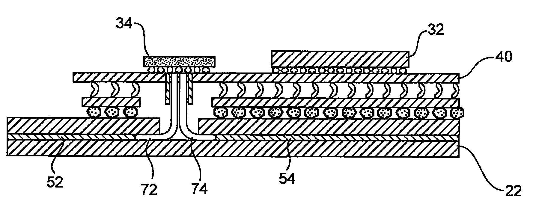
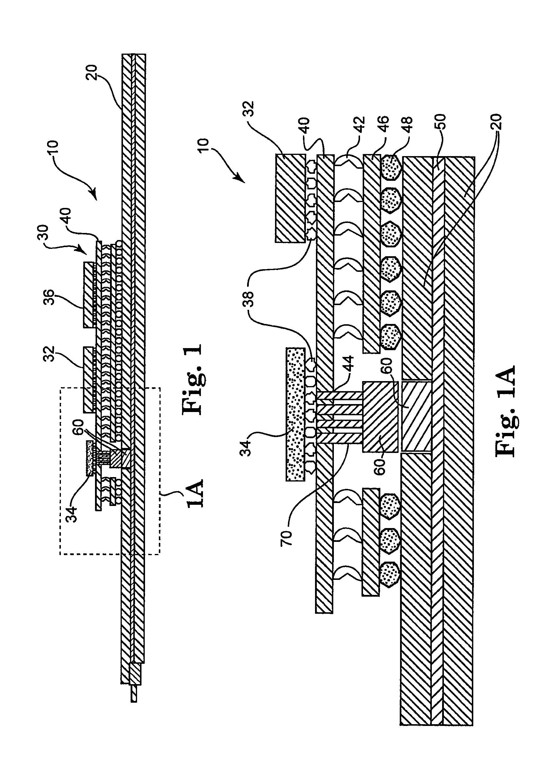
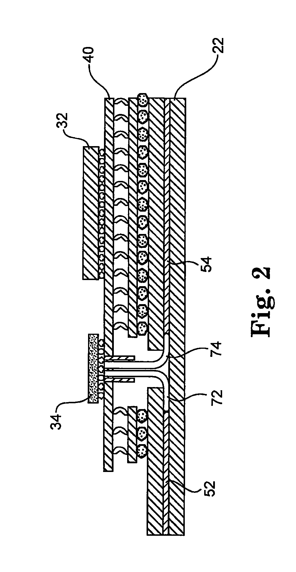
[0013]In an effort to provide significant flexibility during the manufacturing and assembly of optoelectronic systems, the present invention provides a mechanism to more easily interconnect optoelectronic elements to associated waveguides or fibers embedded in printed circuit boards. Generally speaking, the present invention approaches this problem by providing openings in the bottom surface of a chip carrier which are specifically configured to receive fibers for optical coupling.

[0014]Referring now to FIG. 1, one embodiment of this connection methodology is illustrated. Generally speaking, FIG. 1 is a cross-sectional diagram of a circuit assembly 10 which includes a printed circuit board 20 and a multi-chip module 30 attached thereto. Multi-chip module 30 includes a processor chip 32, an optoelectronic chip 34 and a related electrical chip 36 attached to a carrier 40. In this example, additional chips may exist on carrier 40 depending on the particular application. Similarly, the ...


PUM


Abstract

Considerable manufacturing efficiency and flexibility is provided by configuring the lower surface of a chip carrier to include multiple holes specifically designed to receive coupling fibers. By appropriately positioning these holes, the coupling fibers can be aligned with necessary optical elements of optoelectronic chips carried by the chip carrier. Similarly, the opposite end of the fibers can be appropriately configured and positioned for coupling to waveguide structures or fiber optic structures which may be embedded in printed circuit boards. By utilizing an appropriately configured chip carrier, and related fibers, a signal transmission structure is achieved which effectively bridges the gap between a chip carrier and a related printed circuit board.

Description

FIELD OF THE INVENTION[0001]The present invention relates to chip carrier structures which accommodate optoelectronic chips. More specifically, the present invention relates to a chip carrier structure which more easily provides an optical connection mechanism for coupling optoelectronic components to related optical signals carriers embedded or attached to circuit boards.BACKGROUND OF THE INVENTION[0002]With the increasing performance of processors and switching chips, a similar increase in bandwidth requirements for incoming and outgoing data also exists. In certain cases, electrical interconnects can provide bandwidth limitations for microelectronic chips. These limitations are a result of maximum electrical line density and maximum data rates per line. One potential solution to this higher bandwidth requirement is the use of optical components and optical communication connections. Simply stated, optical communications is capable of operating at higher speeds per line, and a hig...

Claims


Application Information

Patent Timeline
Patent Type & Authority Patents(United States)
IPC IPC(8): G02B6/12
CPCG02B6/421H05K1/0274G02B6/43H05K1/141H05K2201/10121H01L2224/16225H01L2924/15311
Inventor DELLMANN, LAURENT A.HORST, FOLKERTOFFREIN, BERT J.
Owner IBM CORP
Why Eureka
Try Eureka