LSI apparatus operated by optical clock

a technology of optical clock and optical clock, which is applied in the direction of optical elements, instruments, generating/distributing signals, etc., can solve the problems of difficult to achieve the operation in synchronism with the logic circuit, the clocks are distributed to the internal circuit parts of the lsi, and the clock distribution is difficult to achieve. the effect of reducing the jitter of the clock distribution

Inactive Publication Date: 2009-02-17
KK TOSHIBA
View PDF9 Cites 7 Cited by
  • Summary
  • Abstract
  • Description
  • Claims
  • Application Information

AI Technical Summary

Benefits of technology

[0009]An object of the present invention is to provide an LSI apparatus operated by an optical clock, which permits optically distributing the clocks, which are subjected to a high speed signal processing, to an LSI and also permits diminishing the clock distribution jitter.

Problems solved by technology

However, the improvement in the performance of the LSI, which is achieved by the miniaturization of the transistors, is accompanied by a serious problem.
The particularly serious problem resides in the distribution of the clocks to the internal circuit parts of the LSI.
To be more specific, the reaching time of the clock signal differs depending on the arranging position of the LSI circuit part so as to make it difficult to achieve the operation in synchronism with the logic circuit.
The particular problem is being made more and more serious in recent years.
Also, in the system using the clock distributing tree, which is disclosed in the Japanese Patent document quoted above, the optical pulses are distributed through a large number of branched portions, with the result that it is difficult to align the wiring length and the light amount thereof for the set pulse and the reset pulse.
It follows that the dependency on the site such that the reaching timing of the set pulse and the reset pulse differs depending on the site is not negligible, with the result that the clock jitter is substantially generated in the entire LSI system.
It should also be noted that a bias drift is generated in the clock signal by the difference in the light amount between the set pulse and the reset pulse so as to give rise to the problem that the jitter is substantially increased by the warp in the width of the clock pulse or the change thereof.

Method used


Image

  • LSI apparatus operated by optical clock
  • LSI apparatus operated by optical clock
  • LSI apparatus operated by optical clock

Examples


first embodiment

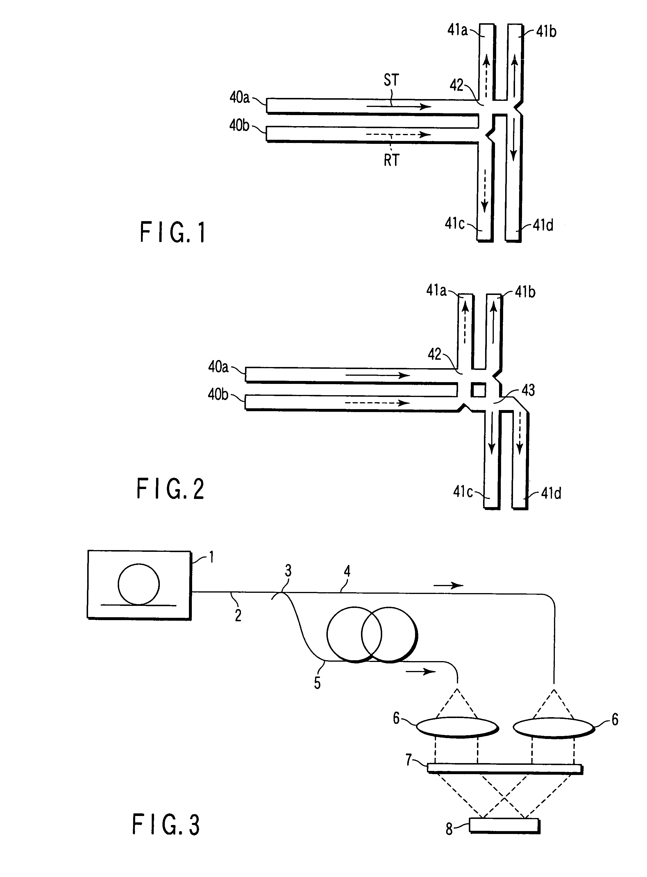
[0058]FIG. 3 schematically shows an optical waveguide arrangement of the LSI system operated by the optical clock according to a first embodiment of the present invention.

[0059]Reference numeral 1 shown in FIG. 3 denotes a short optical pulse source for generating a short optical pulse. The short optical pulse generated from the pulse source 1 is guided by an optical fiber 2, and the guided short optical pulse is divided into two components by an optical divider 3, i.e., a two-branching optical fiber coupler. The two branched components of the short optical pulse are guided by optical fibers 4 and 5, respectively, and collimated by collimate lenses 6. Then, the collimated optical pulse components are incident on a diffraction grating 7. The diffraction grating 7 permits the short optical pulse to be incident on an LSI apparatus, i.e., an LSI chip 8 at a prescribed incident angle. In the system shown in FIG. 3, the optical fiber 5 is set longer than the optical fiber 4 by an amount c...

second embodiment

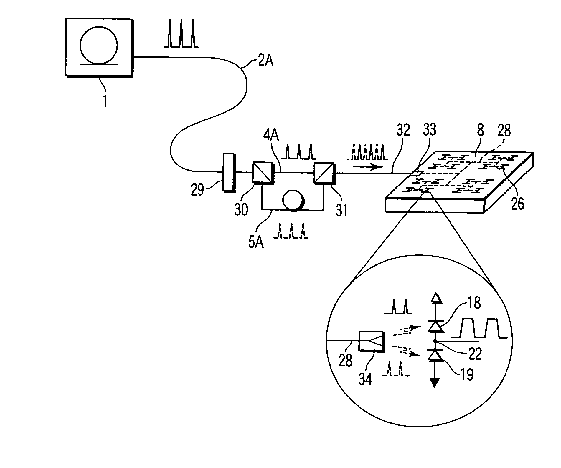
[0080]FIG. 9 schematically shows the construction of an optical clock LSI system according to a second embodiment of the present invention.

[0081]A reference numeral 1 shown in FIG. 9 denotes a short optical pulse source for generating a short optical pulse. In the system shown in FIG. 9, the short optical pulse is guided by an optical fiber 2A while preserving the polarized plane of the short optical pulse that is linearly polarized so as to be incident on a wave plate 29. In the wave plate 29, the linearly polarized light beam is converted into a circularly polarized light beam, and the circularly polarized light beam is separated by a polarized beam splitter 30 acting as a de-multiplexing element into light beam components having polarized planes perpendicular to each other. The light beam component having one of the polarized planes perpendicular to each other is guided by a fiber 4A into a multiplexing element 31 while retaining the polarized plane. Also, the light beam having t...

third embodiment

[0091]FIG. 10 schematically shows the configuration of an optical clock LSI system according to a third embodiment of the present invention.

[0092]A reference numeral 1 shown in FIG. 9 denotes a short optical pulse source. Each of reference numerals 2A, 4A and 5A denotes a polarized beam-preserving optical fiber for preserving the polarizing plane of the optical beam generated from the short pulse optical pulse source 1. A reference numeral 8 denotes an LSI chip, a reference numeral 29 denotes a wave plate, a reference numeral 30 denotes a polarized beam splitter, a reference numeral 31 denotes a multiplexing unit, a reference numeral 32 denotes an optical fiber, and a reference numeral 35 denotes a collimate lens.

[0093]The optical system between the short optical pulse source 1 and the optical fiber 32 is equal in construction and function to the second embodiment described above and, thus, the detailed description thereof is omitted. In the optical clock LSI shown in FIG. 10, a sin...


PUM


Abstract

In an LSI system, a short optical pulse train is guided to an optical divider which divides the short optical pulse train into first and second short optical pulse trains. A retardation of ½ of the pulse period is produced between the first and second short optical pulse trains. The first and second short optical pulse trains are guided to first and second photodiodes on an LSI chip and are converted in the first and second electric current pulse trains, respectively. The first and second electric current pulse trains are supplied to an electrical clock output terminal electrically connected to the first and second photodiodes so that the electrical clock output terminals generates an electric clock pulse.

Description

CROSS-REFERENCE TO RELATED APPLICATIONS[0001]This is a Continuation Application of PCT Application No. PCT / JP2005 / 021182, filed Nov. 11, 2005, which was published under PCT Article 21(2) in English.[0002]This application is based upon and claims the benefit of priority from prior Japanese Patent Application No. 2004-327708, filed Nov. 11, 2004, the entire contents of which are incorporated herein by reference.BACKGROUND OF THE INVENTION[0003]1. Field of the Invention[0004]The present invention relates to an LSI apparatus operated by an optical clock, particularly, to an LSI apparatus operated by an optical clock, in which a clock is optically distributed to an LSI chip for processing a signal at a high speed so as to convert the optical clock into an electric clock for operating the LSI.[0005]2. Description of the Related Art[0006]With improvement of the performance of an electronic device such as a bipolar transistor or an electric field effect transistor (FET), the operating speed...

Claims


Application Information

Patent Timeline
Patent Type & Authority Patents(United States)
IPC IPC(8): G02B6/12H04B10/04H04B10/12G06F1/04G06F1/10H01L27/15H01L31/12
CPCG02B6/125G06F1/105G02B6/4214G06F1/08G06F1/10
Inventor FURUYAMA, HIDETO
Owner KK TOSHIBA
Why Eureka
Try Eureka