

Decreasing the etch rate of silicon nitride by carbon addition
a technology of silicon nitride and carbon addition, which is applied in the manufacture of semiconductor/solid-state devices, basic electric elements, electric devices, etc., can solve the problems of insufficient masking of the underlying layer, the thickness of the resist layer cannot be increased, and the integrated circuit has evolved into complex devices
- Summary
- Abstract
- Description
- Claims
- Application Information
AI Technical Summary
Benefits of technology
Problems solved by technology
Method used
Image

Examples
example 1
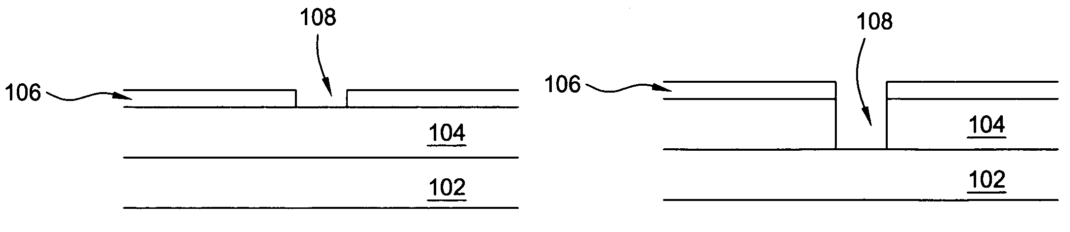
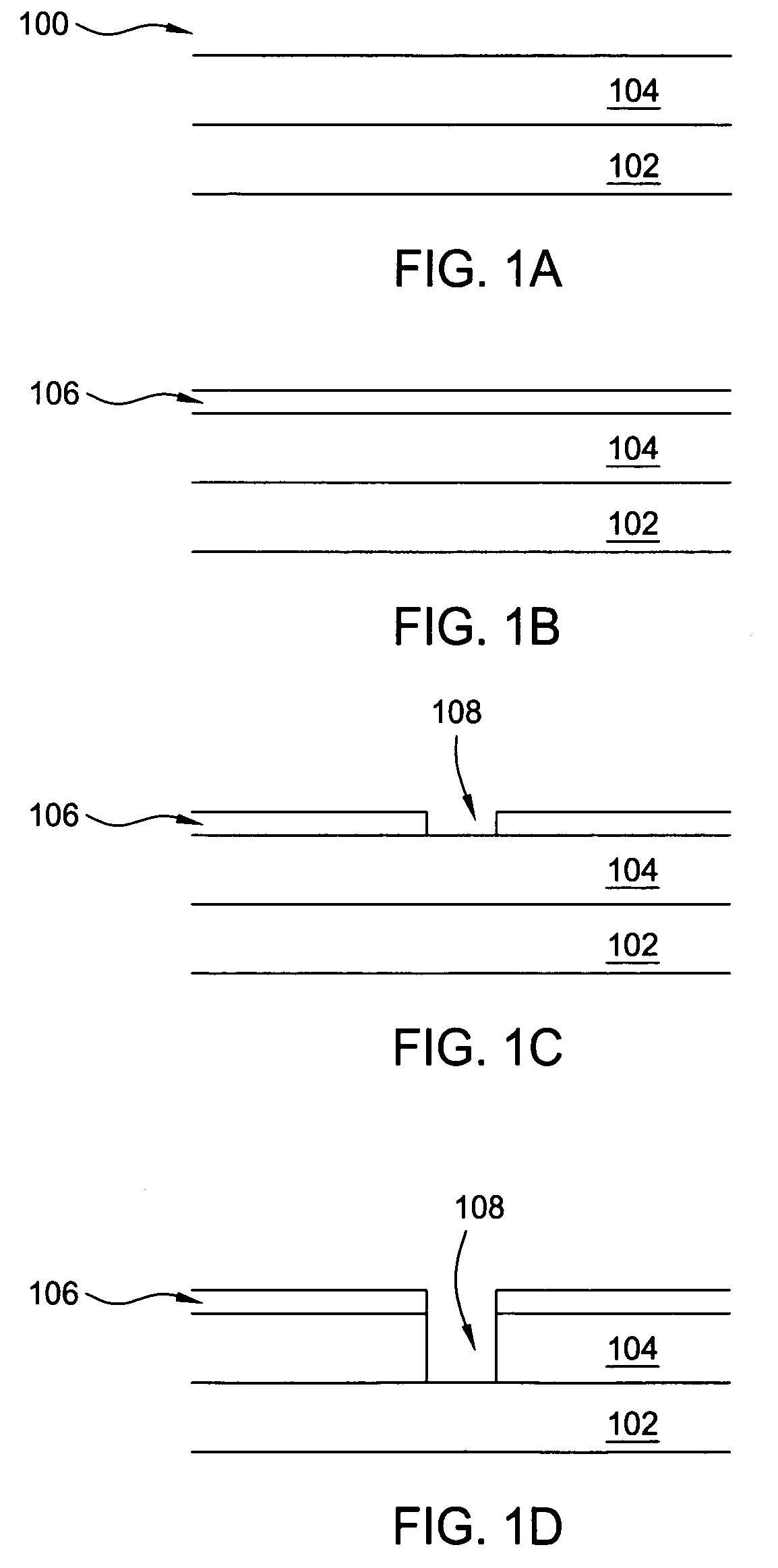
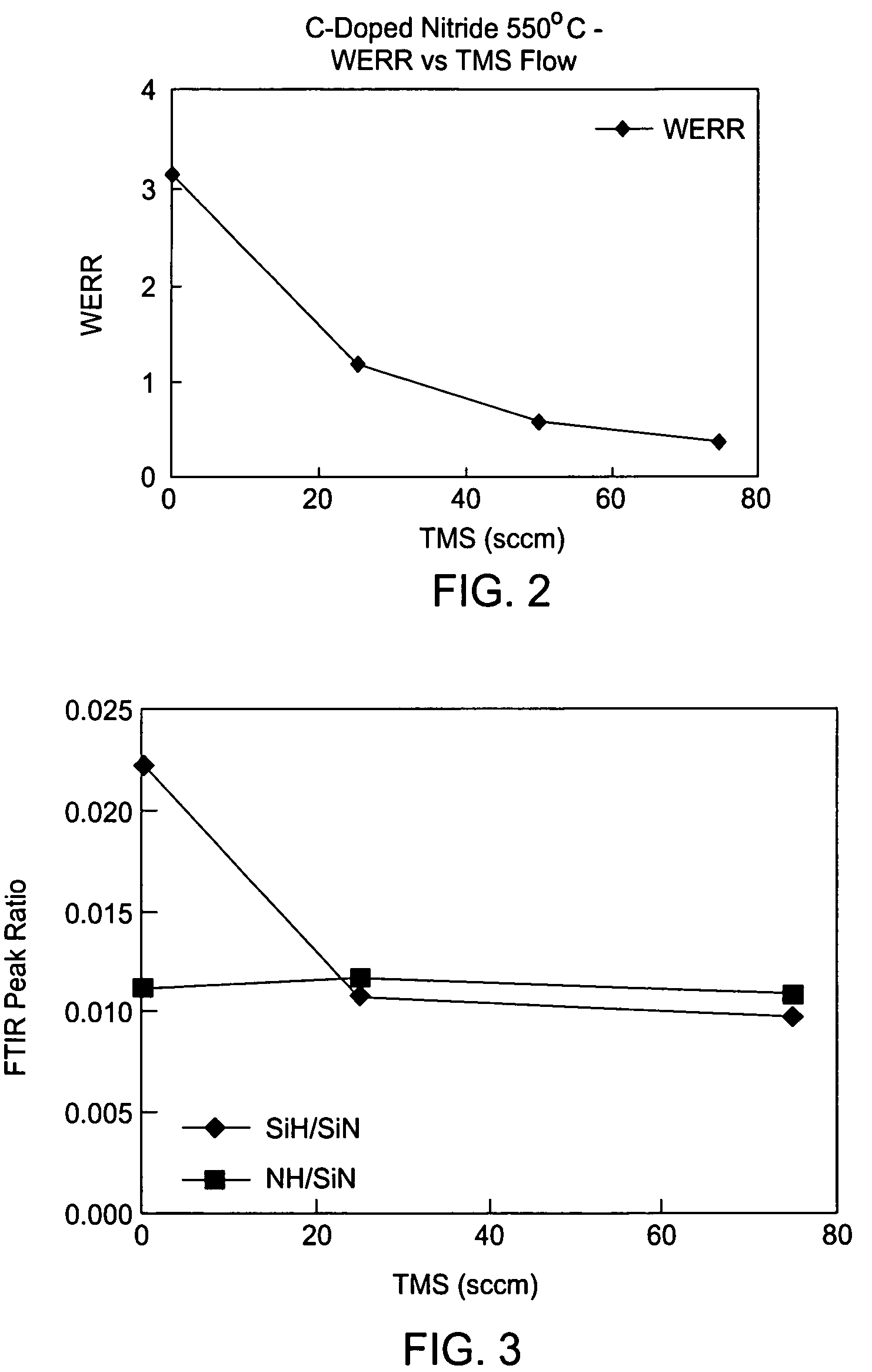
[0045]A carbon-doped silicon nitride layer was deposited on a substrate at about 2 Torr, a temperature of about 550° C., and a spacing of about 480 mils. The following process gases and flow rates were used: trimethylsilane at 50 sccm; silane at 340 sccm; ammonia at 3200 sccm; and nitrogen at 4000 sccm. The trimethylsilane, silane, and ammonia were reacted in the presence of RF power applied to a showerhead electrode in the chamber at 60 W and a frequency of 13.56 MHz and to the substrate support at 50 W and a frequency of 350 kHz for plasma enhanced deposition of a carbon-doped silicon nitride layer. The carbon-doped silicon nitride layer had a wet etch rate of 2.0 Å / min in 100:1 diluted hydrofluoric acid (HF), a wet etch rate ratio (WERR) of 0.6, a wet etch rate uniformity of 4.5%, and a dry etch selectivity ratio of 1.1. The dry etch selectivity ratio is the ratio of the over etch depth of the film of interest vs. thermal nitride. Other film properties that were obtained were a w...
example 2
[0046]A silicon nitride layer was deposited on a substrate at about 2 Torr, a temperature of about 550° C., and a spacing of about 480 mils. The following process gases and flow rates were used: silane at 340 sccm; ammonia at 3200 sccm; and nitrogen at 4000 sccm. The silane and ammonia were reacted in the presence of RF power applied to a showerhead electrode in the chamber at 60 W and a frequency of 13.56 MHz and to the substrate support at 50 W and a frequency of 350 kHz for plasma enhanced deposition of a silicon nitride layer. The silicon nitride layer had a wet etch rate of 6.4 Å / min in 100:1 diluted hydrofluoric acid (HF), a wet etch rate uniformity of 2.6%, and a dry etch selectivity ratio of 1.25. Other film properties that were obtained were a within wafer thickness uniformity of 0.98%, a refractive index of 2.0077, a stress of −807 MPa, a leakage current of 2.0×10⁻⁹ at 2 MV / cm, and a breakdown voltage of 8.4 MV / cm.
[0047]The silicon nitride layer was then UV post-treated fo...
PUM
| Property | Measurement | Unit |
|---|---|---|
| temperature | aaaaa | aaaaa |
| temperature | aaaaa | aaaaa |
| temperatures | aaaaa | aaaaa |
Abstract
Description
Claims
Application Information