Trench-gate field effect transistors and methods of forming the same

a field effect transistor and field effect transistor technology, applied in semiconductor devices, diodes, electrical apparatus, etc., can solve the problems of limiting the improvement of rdson, and limiting the improvement of several performance parameters such as breakdown voltage and transistor ruggedness

Inactive Publication Date: 2009-03-17
SEMICON COMPONENTS IND LLC
View PDF11 Cites 97 Cited by
  • Summary
  • Abstract
  • Description
  • Claims
  • Application Information

AI Technical Summary

Benefits of technology

[0013]In accordance with another embodiment of the invention, a field effect transistor includes a body region of a first conductivity type in a semiconductor region of a second conductivity type. A gate trench extends through the body region and terminating within the semiconductor region. A source region of the second conductivity type is in the body region adjacent the gate trench such that the source region and an interface between the body region and the semiconductor region define a channel region extending along the gate trench sidewall. A channel enhancement region of the second conductivity type is adjacent the gate trench. The channel enhancement region partially extends into a lower portion of the channel region to thereby reduce a resistance of the channel region.
[0016]In accordance with another embodiment of the invention, a field effect transistor is formed as follows. A trench is formed in a semiconductor region. A shield electrode is formed in the trench. An angled sidewall implant of impurities of the first conductivity type is performed to form a channel enhancement region adjacent the trench. A body region of a second conductivity type is formed in the semiconductor region. A source region of the first conductivity type is formed in the body region such that the source region and an interface between the body region and the semiconductor region defining a channel region extending along the gate trench sidewall. The channel enhancement region partially extends into a lower portion of the channel region to thereby reduce a resistance of the channel region.

Problems solved by technology

One drawback of both the single gate transistor 100 and dual gate transistor 200, however, is that the drift region contributes up to about 40% of the total Rdson, significantly limiting improvements in Rdson.
Another drawback of trench-gate transistors 100 and 200 is that the high electric field at the bottom of the trench due to the bottom trench curvature, limits improving several performance parameters such as breakdown voltage and transistor ruggedness.
However, such integration typically requires a complex process technology with many process and mask steps.

Method used


Image

  • Trench-gate field effect transistors and methods of forming the same
  • Trench-gate field effect transistors and methods of forming the same
  • Trench-gate field effect transistors and methods of forming the same

Examples


Embodiment Construction

[0036]The process sequence represented by the cross-section views in FIGS. 13A-13L is an exemplary process for forming a dual gate trench MOSFET in accordance with an embodiment of the invention. This process sequence will be used as the base process which will be modified to include various process modules for forming the different cell structures described below. Note that the process modules described herein may also be integrated with other base processes, and as such are not limited to the process depicted by FIGS. 13A-13L. The process sequence of FIGS. 13A-13L is described next.

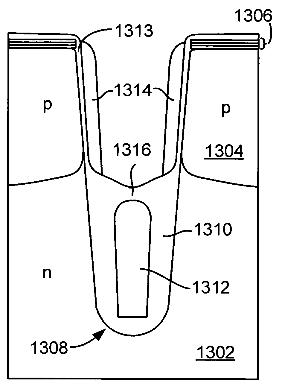
[0037]In FIG. 13A, an n-type epitaxial layer 1302 is formed over a heavily doped n-type substrate (not shown). Dopants of p-type conductivity are implanted to form a body region 1304 in epitaxial layer 1302. A hard mask 1306, e.g., comprising oxide-nitride-oxide (ONO) composite layer, is used to define and etch trenches 1308 extending through body region 1304 and into epitaxial layer 1302.

[0038]In FIG. ...


PUM


Abstract

A method for forming a shielded gate field effect transistor includes the following steps. Trenches extending into a silicon region are formed using a mask that includes a protective layer. A shield dielectric layer lining sidewalls and bottom of each trench is formed. A shield electrode is formed in a bottom portion of each trench. Protective spacers are formed along upper sidewalls of each trench. An inter-electrode dielectric is formed over the shield electrode. The protective spacers and the protective layer of the mask prevent formation of inter-electrode dielectric along the upper sidewalls of each trench and over mesa surfaces adjacent each trench. A gate electrode is formed in each trench over the inter-electrode dielectric.

Description

CROSS-REFERENCES TO RELATED APPLICATIONS[0001]This application claims the benefit of U.S. Provisional Application No. 60 / 685,727, filed on May 26, 2005, which is incorporated herein by reference in its entirety for all purposes.[0002]The commonly assigned U.S. application No. 11 / 026,276, filed Dec. 29, 2004 is incorporated herein by reference in its entirety for all purposes.BACKGROUND OF THE INVENTION[0003]The present invention relates to semiconductor power devices, and more particularly to improved trench-gate power devices and methods of manufacturing the same.[0004]FIG. 1 is a cross section view of a conventional trench-gate MOSFET 100 which has known physical and performance characteristics and limitations such as cell pitch, break down voltage capability, on-resistance (Rdson), transistor ruggedness. Trench gate 105 extends through P-well 106 and terminates in N-epi region 104. Trench gate 105 includes a gate dielectric 114 lining the trench sidewalls and bottom, and a recess...

Claims


Application Information

Patent Timeline
Patent Type & Authority Patents(United States)
IPC IPC(8): H01L21/336
CPCH01L29/407H01L29/66727H01L29/66734H01L29/7806H01L29/7811H01L29/7813H01L29/872H01L29/66666H01L29/7827H01L21/26586H01L29/0878H01L29/402H01L29/41766H01L29/4236H01L29/42368
Inventor YILMAZ, HAMZACALAFUT, DANIELKOCON, CHRISTOPHER BOGUSLAWSAPP, STEVEN P.PROBST, DEAN E.KRAFT, NATHAN L.GREBS, THOMAS E.RIDLEY, RODNEY S.DOLNY, GARY M.MARCHANT, BRUCE D.YEDINAK, JOSEPH A.
Owner SEMICON COMPONENTS IND LLC
Why Eureka
Try Eureka