High dielectric film and related method of manufacture

a dielectric film, high-dielectric technology, applied in the direction of coating, metallic material coating process, chemical vapor deposition coating, etc., can solve the problems of high-dielectric film, semiconductor field-effect transistor (mosfet) devices suffer from a number of shortcomings, and are still not suitable for a transistor in a highly miniaturized device, so as to improve leakage current characteristics

Active Publication Date: 2009-04-21
SAMSUNG ELECTRONICS CO LTD
View PDF9 Cites 59 Cited by
  • Summary
  • Abstract
  • Description
  • Claims
  • Application Information

AI Technical Summary

Benefits of technology

[0013]Embodiments of the present invention provide several methods of forming a high dielectric film by atomic layer deposition. Several of these embodiments address the need to improve leakage current characteristics by reducing defects such as carbon within the high dielectric film and precisely controlling the quantity of nitrogen within the high dielectric film. In addition, embodiments of the present invention also provide semiconductor devices including a high dielectric film formed by atomic layer deposition.

Problems solved by technology

Unfortunately, conventional high dielectric films used as gate insulating layers in metal-oxide semiconductor field-effect transistor (MOSFET) devices suffer from a number of shortcomings.
Although this approach is an improvement over the HfO2 layer, it is still not adequate for a transistor in a highly miniaturized device.
One problem with using the annealing technique to form the nitride oxide layer is that it does not allow precise control over the profile of nitrogen within the nitride oxide layer.
In addition, the annealing technique must be performed as a separate process in addition to the other processes used to form the high dielectric film, thereby increasing the complexity of the methods used to form the high dielectric film.
One of the problems with the new methods is that N-bonds may not readily form in the HfSiON layer within a thin high dielectric film.
The carbon remaining in the HfSiO layer tends to degrade the electrical characteristics of the layer.

Method used


Image

  • High dielectric film and related method of manufacture
  • High dielectric film and related method of manufacture
  • High dielectric film and related method of manufacture

Examples


Embodiment Construction

[0024]Exemplary embodiments of the invention are described below with reference to the corresponding drawings. These embodiments are presented as teaching examples. The actual scope of the invention is defined by the claims that follow.

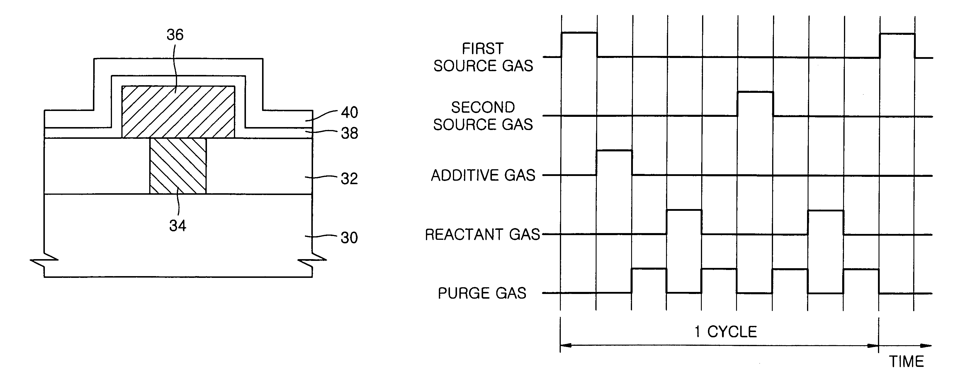
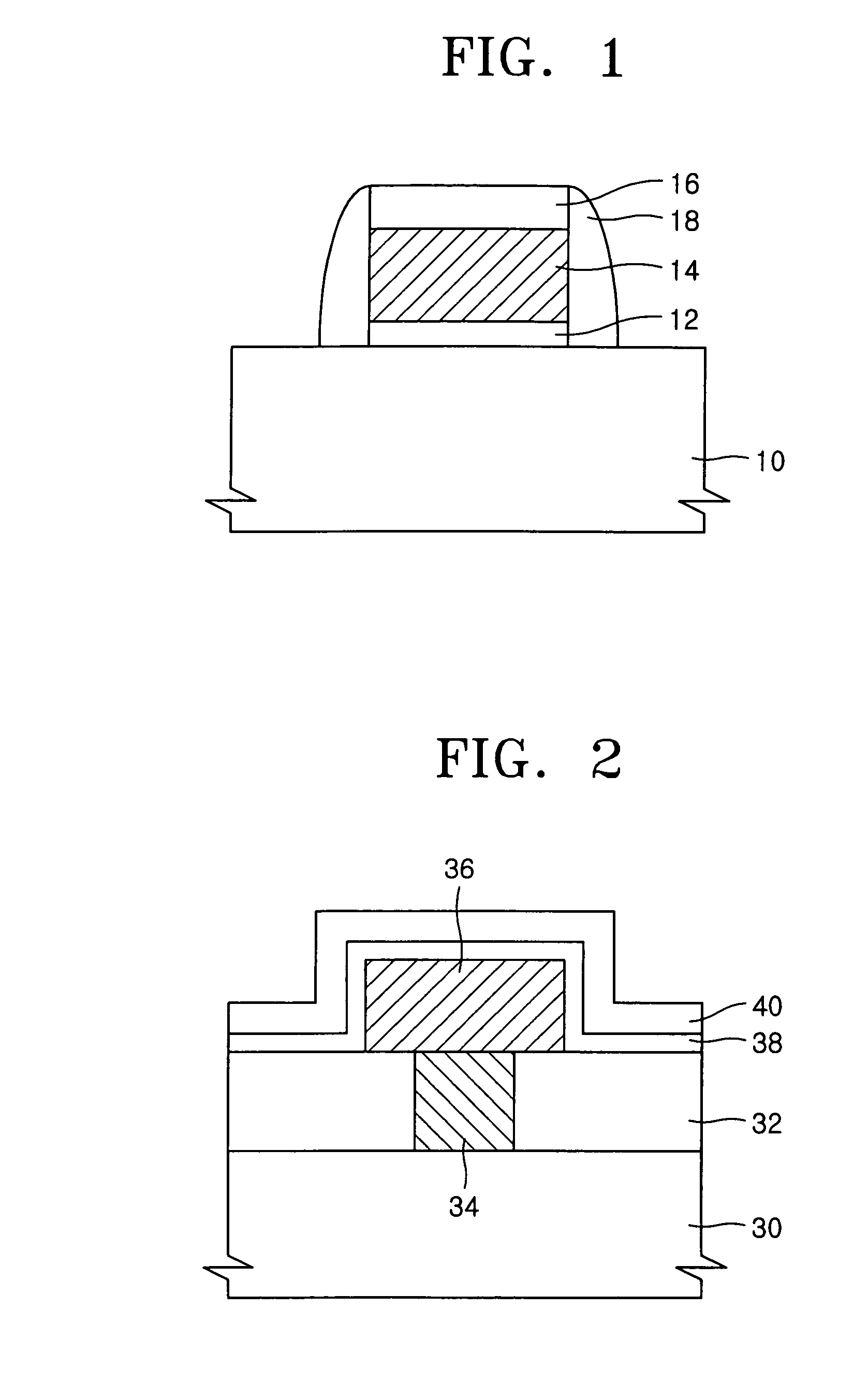
[0025]FIG. 1 is a sectional view of a semiconductor device including a gate structure fabricated according to an embodiment of the present invention. Referring to FIG. 1, a gate dielectric film layer, a gate electrode material layer, a gate mask layer, and a mask pattern are successively formed on a semiconductor substrate 10. Then, the gate mask layer, the gate electrode material layer, and the dielectric film layer are etched using the mask pattern as an etch mask to form a gate structure including a gate dielectric film 12, a gate electrode material 14, and a gate mask 16, sequentially stacked on semiconductor substrate 10. After the gate structure is formed, a gate spacer 18 comprising a material such as silicon nitride or silicon oxide is formed ...


PUM

PropertyMeasurementUnit
dielectric constantaaaaaaaaaa
timeaaaaaaaaaa
timeaaaaaaaaaa

Abstract

A method of forming a high dielectric film for a semiconductor device comprises supplying a first source gas to a reaction chamber during a first time interval, supplying a first reactant gas to the reaction chamber during a second time interval after the first time interval, supplying a second source gas to the reaction chamber for a third time interval after the second time interval, supplying a second reactant gas to the reaction chamber for a fourth time interval after the third time interval, and supplying an additive gas including nitrogen to the reaction chamber during a fifth time interval.

Description

BACKGROUND OF THE INVENTION[0001]1. Field of the Invention[0002]Embodiments of the present invention relate generally to a dielectric film for a semiconductor device. More particularly, embodiments of the invention relate to a high dielectric film formed by Atomic Layer Deposition (ALD), and related methods of manufacture.[0003]A claim of priority is made to Korean Patent Application No. 10-2005-0020134, filed on Mar. 10, 2005, the disclosure of which is hereby incorporated reference in its entirety.[0004]2. Description of Related Art[0005]Semiconductor device manufacturers are continually striving to increase the integration density and capacity of semiconductor devices such as computer memories and other electronic data processing elements. As the integration density and capacity of the devices increases, materials with a higher dielectric constant must be used to form gate dielectric films and capacitor dielectric films in the devices. Such films formed with materials having a hi...

Claims


Application Information

Patent Timeline
Patent Type & Authority Patents(United States)
IPC IPC(8): H01L21/76
CPCC23C16/308C23C16/45531H01L21/3141H01L21/3145H01L21/31645H01L21/02274H01L21/02142H01L21/0228H01L21/02194H01L21/205H01L21/31
Inventor PARK, HONG-BAESHIN, YU-GYUNKANG, SANG-BOM
Owner SAMSUNG ELECTRONICS CO LTD
Why Eureka
Try Eureka