Method of fabricating optical device caps

a technology of optical devices and optical caps, applied in semiconductor devices, semiconductor/solid-state device details, electrical apparatus, etc., can solve the problem that optical device caps cannot have good penetrability, and achieve the effect of no contamination, high penetrability, and good penetrability

Inactive Publication Date: 2009-05-05
TOUCH MICRO SYST TECH
View PDF2 Cites 5 Cited by
  • Summary
  • Abstract
  • Description
  • Claims
  • Application Information

AI Technical Summary

Benefits of technology

[0007]It is therefore an object of the present invention to provide a method of fabricating optical device caps so as to have a good hermetic sealing, good penetrability and wafer level packaging.
[0009]The method of fabricating optical device caps of the present invention uses a specific designed plate and an anodic bonding process to provide a glass wafer having clearness, high penetrability and no contamination. Therefore, the problem of having the sodium attached on the glass wafer that cannot be cleaned is solved, and the optical device caps can have a good penetrability.

Problems solved by technology

However, the sodium atoms will be attached to the surface of the glass wafer 14, and the sodium atoms cannot be removed by cleaning in the following process so that the optical device caps cannot have good penetrability.

Method used


Image

  • Method of fabricating optical device caps
  • Method of fabricating optical device caps
  • Method of fabricating optical device caps

Examples


Embodiment Construction

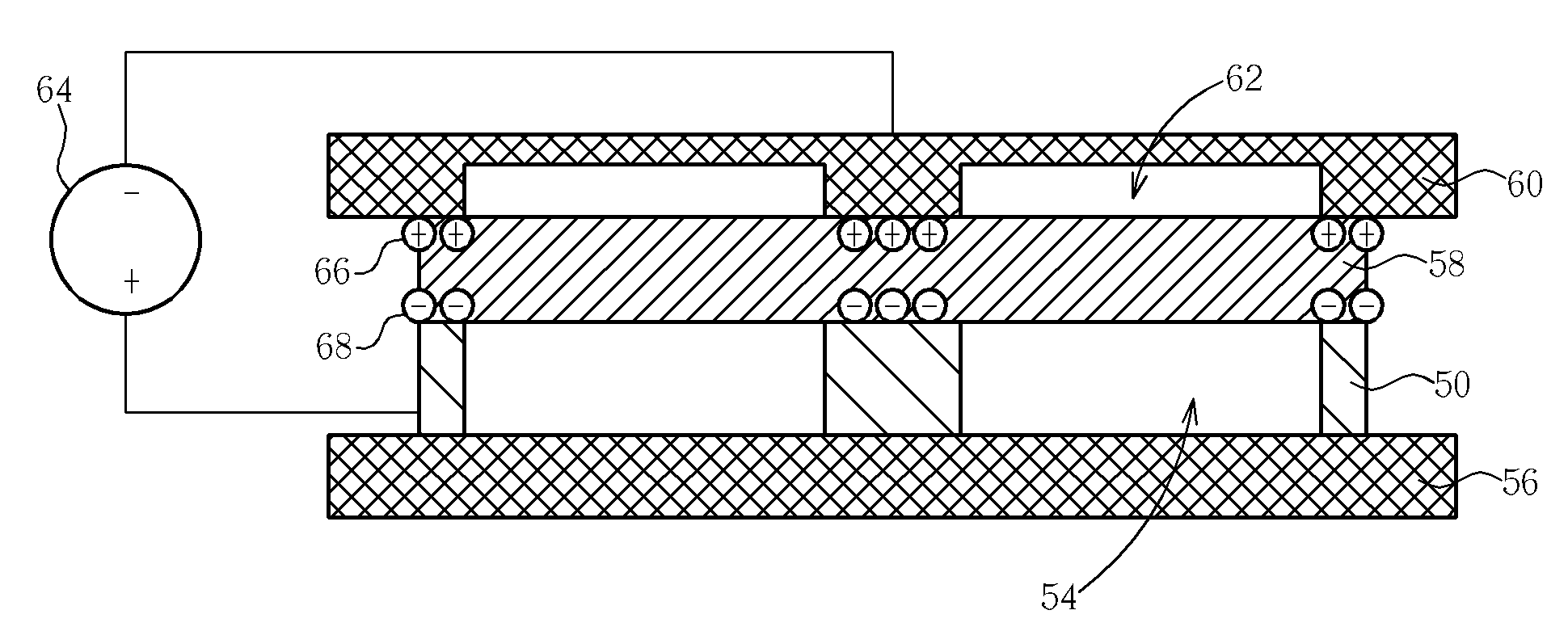
[0015]Please refer to FIG. 5 through FIG. 11. FIG. 5 through FIG. 11 are schematic diagrams illustrating a method of fabricating optical device caps. As shown in FIG. 5, a wafer 50, such as a silicon wafer, is provided, and then, a thinning process is performed to thin the wafer 50 to a required thickness. The thinning process includes a grinding process, a chemical mechanical polishing process, a plasma thinning process or a combination thereof. As shown in FIG. 6, a lithographic process forms a photoresist pattern 52, and then, regarding the photoresist pattern 52 as a mask, an etching process is performed to etch through a part of the wafer 50 not covered by the photoresist pattern 52 so that a plurality of through holes 54 is formed in the wafer 50. The etching process can be a dry etching process, such as a deep reactive ion etching (DRIE) process. As shown in FIG. 7, the photoresist pattern 52 is subsequently removed, and then, a clean process is performed.

[0016]As shown in FI...


PUM


Abstract

A wafer having a plurality of through holes is provided, and a glass wafer is disposed on the wafer. A plate having a plurality of concave cavities is disposed on the glass wafer, wherein the concave cavities corresponding to the through holes of the wafer so that a part of the plate corresponding to the through holes is not in contact with the glass wafer. A voltage source is provided, and two electrodes thereof respectively have electrical connections to the wafer and the plate. The wafer and the glass wafer are bonded to each other by the anodic bonding method so that a plurality of optical device caps are formed.

Description

BACKGROUND OF THE INVENTION[0001]1. Field of the Invention[0002]The present invention relates to a method of fabricating optical device caps, and more particularly, to a method of fabricating optical device caps so as to provide a good hermetic sealing, good penetrability and be able to package in wafer level.[0003]2. Description of the Prior Art[0004]In manufacturing processes, the microelectromechanical products with various kinds of applications and types will have different packaging processes. A wafer level package (WLP) is a semiconductor package in which the size of a finished package is similar to or slightly larger than a semiconductor die. After completion of all test processes and assembly processes or packaging processes, individual semiconductor packages are separated from a wafer having a plurality of semiconductor dies. Therefore WLP not only decreases a size of a memory module, but also satisfies a demand for high density.[0005]Please refer to FIG. 1 through FIG. 3. ...

Claims


Application Information

Patent Timeline
Patent Type & Authority Patents(United States)
IPC IPC(8): H01L21/00
CPCH01L31/0203H01L31/18
Inventor TSAI, CHUN-WEI
Owner TOUCH MICRO SYST TECH
Why Eureka
Try Eureka