

Method for fabricating capacitor in semiconductor device using hafnium terbium oxide dielectric layer
a technology of hafnium terbium oxide and dielectric layer, which is applied in the direction of coatings, transistors, chemical vapor deposition coatings, etc., can solve the problems of limited capacitance of capacitors, leakage currents in the 5 /sub>dielectric layer, and difficulty in securing depth of focus during the subsequent photo-exposure process, etc., to achieve the effect of improving the reliability of the dielectric layer
- Summary
- Abstract
- Description
- Claims
- Application Information
AI Technical Summary
Benefits of technology
Problems solved by technology
Method used
Image

Examples
Embodiment Construction
[0014]A method for fabricating a capacitor in a semiconductor device in accordance with a preferred embodiment of the present invention will be described in detail with reference to the accompanying drawings.
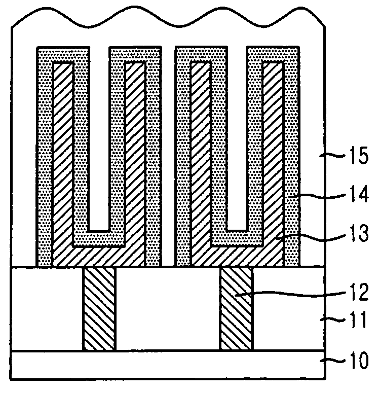
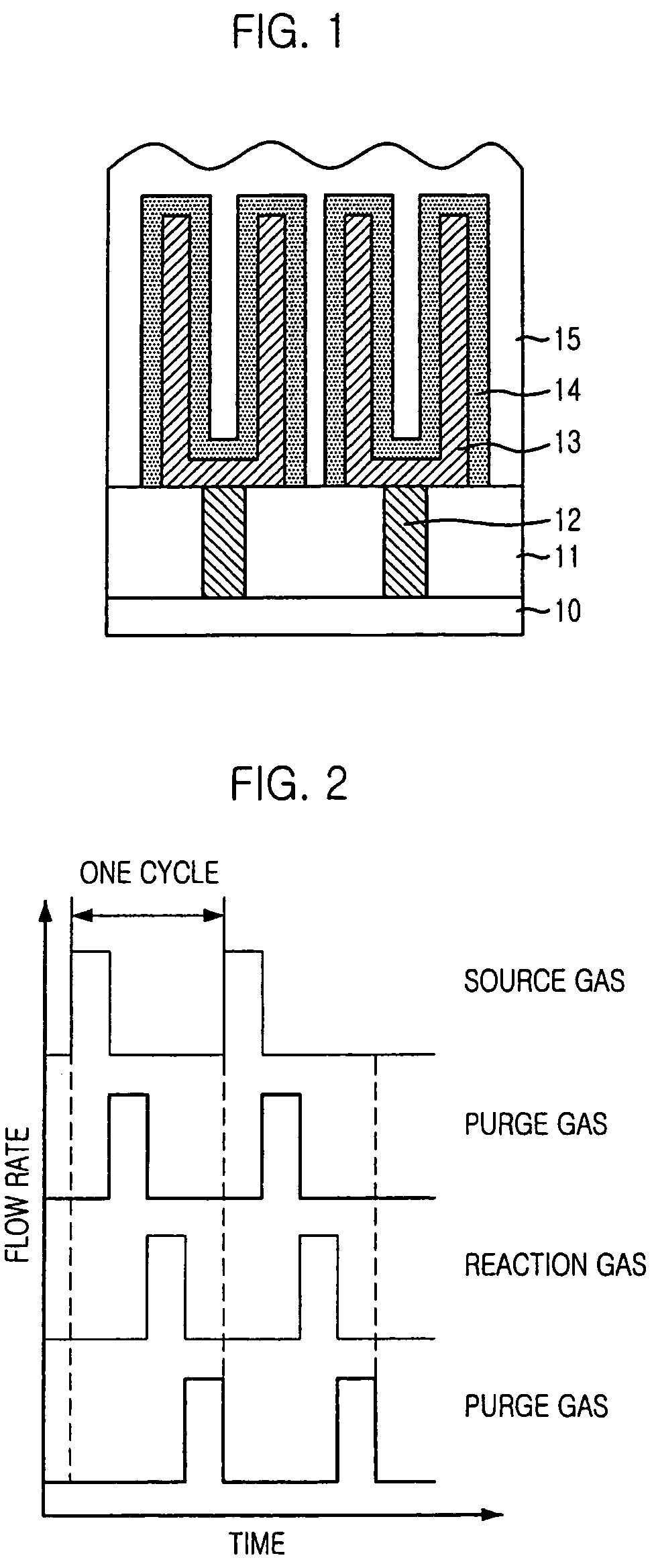
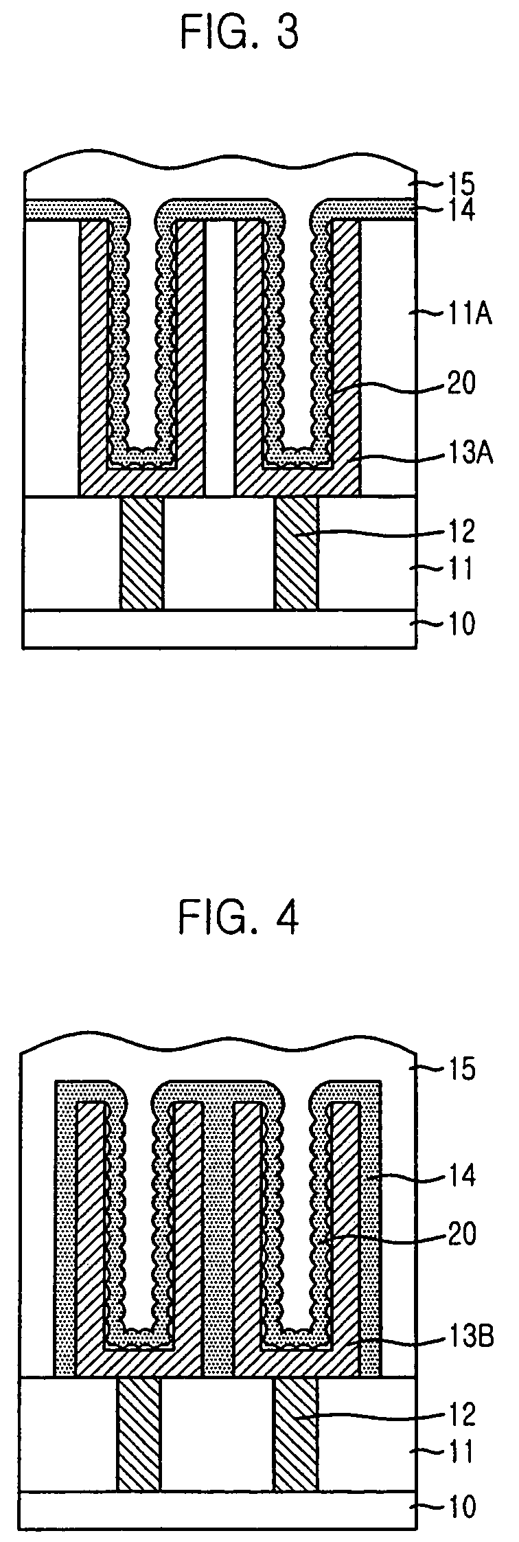
[0015]FIG. 1 is a cross-sectional view illustrating a method for fabricating a cylindrical capacitor in accordance with a first embodiment of the present invention.
[0016]As shown, an inter-layer insulation layer 11 made of silicon dioxide (SiO2) is formed on a semi-finished substrate 10. Although not illustrated, the semi-finished substrate 10 is provided with various device elements such as transistors and bit lines by performing predetermined processes for forming such device elements. Then, the inter-layer insulation layer 11 is etched to form contact holes 12A exposing predetermined portions of the substrate 10. A conductive material is deposited into the contact holes 12A and on the inter-layer insulation layer 11 until the contact holes 12A are filled with the conductive m...
PUM
| Property | Measurement | Unit |
|---|---|---|
| concentration | aaaaa | aaaaa |
| concentration | aaaaa | aaaaa |
| temperature | aaaaa | aaaaa |
Abstract
Description
Claims
Application Information