Semiconductor device and manufacturing method thereof

a technology of semiconductors and manufacturing methods, applied in the direction of semiconductor devices, basic electric elements, electrical appliances, etc., can solve the problems of heavy burden on manufacturing costs and manufacturing processes, and achieve the effect of reducing manufacturing time and manufacturing costs

Inactive Publication Date: 2009-06-02
SEMICON ENERGY LAB CO LTD
View PDF13 Cites 8 Cited by
  • Summary
  • Abstract
  • Description
  • Claims
  • Application Information

AI Technical Summary

Benefits of technology

[0031]By the present invention, different individual data such as ID numbers can be easily given to individual semiconductor devices capable of wireless communication that use ICs.
[0032]In this way, reduction of manufacturing time and manufacturing cost of a semiconductor device capable of wireless communication that uses an IC can be realized.

Problems solved by technology

However, the mask ROM (hereinafter simply referred to as a ROM) can only write data at the time of manufacturing.
Thus, when the individual data such as the ID numbers are formed to be all different, a heavy burden is imposed on manufacturing cost and the manufacturing process.

Method used


Image

  • Semiconductor device and manufacturing method thereof
  • Semiconductor device and manufacturing method thereof
  • Semiconductor device and manufacturing method thereof

Examples


embodiment mode 1

[0060]Embodiment modes and embodiments of the present invention will be described with reference to the drawings. It is easily understood by those skilled in the art that various changes may be made in forms and details without departing from the spirit and the scope of the invention. Therefore, the present invention should not be limited to the descriptions of the embodiment modes and embodiments below. In addition, in the following drawings, the same reference numerals are commonly given to the same components or components having a similar function, and the repetitive description thereof is omitted.

[0061]Embodiment Mode 1 will be described with reference to FIG. 1, FIGS. 5A to 5C, FIGS. 6A to 6C, FIGS. 7A to 7C, FIGS. 8A and 8B, FIGS. 9A and 9B, FIG. 10, FIG. 11, FIG. 12, FIG. 13, FIG. 14, and FIG. 15.

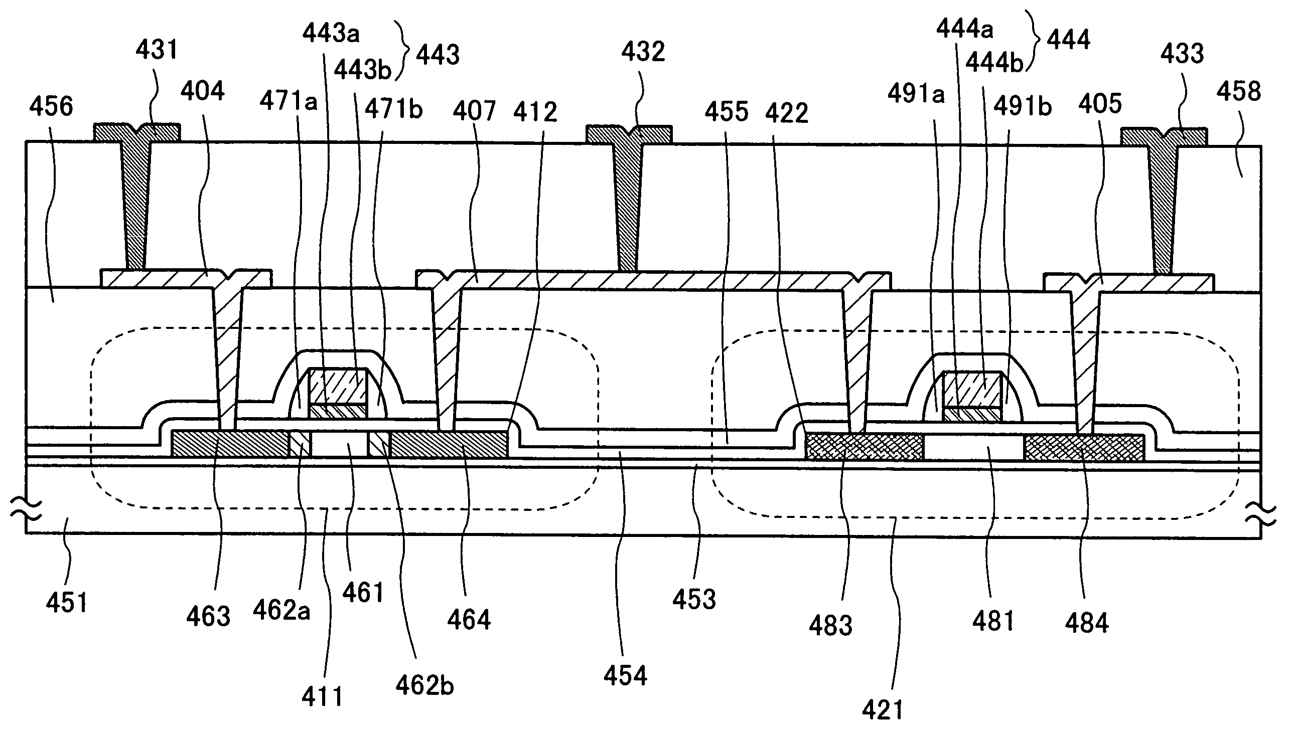
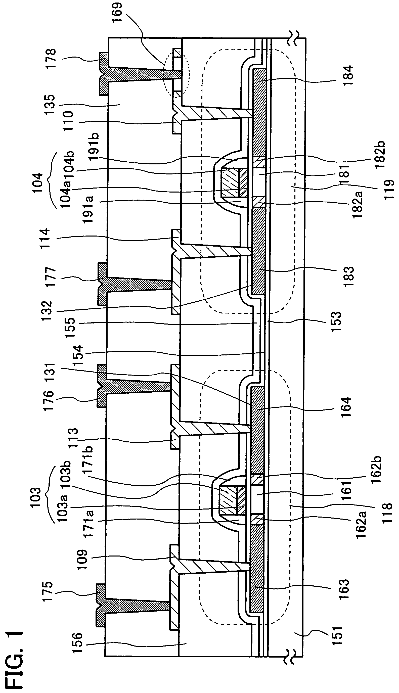
[0062]FIG. 10 is a circuit diagram of a mask ROM and includes a column decoder 15, a row decoder 16, a memory cell array 11 including n-channel TFTs 118 to 121, bit lines (data line...

embodiment mode 2

[0175]In Embodiment Mode 2, a manufacturing process of TFTs of a memory cell array and TFTs of a logic circuit over the same substrate will be described with reference to FIGS. 16A to 16D, FIGS. 17A to 17C, FIGS. 18A to 18C, FIGS. 19A and 19B, and FIGS. 20A and 20B.

[0176]First, as shown in FIG. 16A, a base film 602 is formed over a substrate 601. As the substrate 601, a glass substrate of barium borosilicate glass, alumino borosilicate glass, or the like, a quartz substrate, a stainless-steel substrate, an SOI (Silicon on Insulator) substrate which is formed by formation of a single crystalline semiconductor layer on an insulating surface, or the like can be used. Also, a substrate including a synthetic resin having flexibility such as acrylic or plastic represented by poly(ethylene terephthalate) (PET), poly(ether sulfone) (PES), or poly(ethylene Naphthalate) (PEN) can be used. A case of using a glass substrate as the substrate 601 will be described below.

[0177]The base film 602 is...

embodiment mode 3

[0242]Embodiment Mode 3 will describe a manufacturing method of a semiconductor device capable of wireless communication that uses an IC, which is different from those in Embodiment Modes 1 and 2 with reference to FIG. 14, FIGS. 21A and 21B, FIGS. 22A and 22B, and FIG. 23. In this embodiment mode, components which are the same as those in Embodiment Mode 1 or Embodiment Mode 2 are denoted by the same reference numerals.

[0243]First, in accordance with the description in Embodiment Mode 2, a semiconductor device shown in FIG. 20B is manufactured. Note that instead of the base film 602, a separation layer 802, a first base film 803, and a second base film 804 are formed.

[0244]The separation layer 802 is formed of an amorphous semiconductor film, a polycrystalline semiconductor film, or a semi-amorphous semiconductor film. For example, a layer mainly containing silicon such as amorphous silicon, polycrystalline silicon, single-crystalline silicon, or semi-amorphous silicon. The separati...


PUM


Abstract

The semiconductor device includes a thin film transistor; a first interlayer insulating film over the thin film transistor; a first electrode electrically connected to one of a source region and a drain region, over the first interlayer insulating film; a second electrode electrically connected to the other of the source region and the drain region; a second interlayer insulating film formed over the first interlayer insulating film, the first electrode, and the second electrode; a first wiring electrically connected to one of the first electrode and the second electrode, on the second interlayer insulating film; and a second wiring not electrically connected to the other of the first electrode and the second electrode, on the second interlayer insulating film; in which the second wiring is not electrically connected to the other of the first electrode and the second electrode by a separation region formed in the second interlayer insulating film.

Description

BACKGROUND OF THE INVENTION[0001]1. Field of the Invention[0002]The present invention relates to semiconductor devices capable of communication with the use of contactless means such as wireless communication, and a manufacturing method thereof. In particular, the present invention relates to a semiconductor device that is formed over an insulating substrate of glass, plastic, or the like and a manufacturing method thereof.[0003]2. Description of the Related Art[0004]With development of computer technologies and improvement of image recognition technologies, data identification methods utilizing a medium such as bar codes have spread widely and have been used for identification of product data and the like. It is expected that the amount of data to be identified will further increase in the future. On the other hand, data identification utilizing bar codes is disadvantageous in that a bar code reader is required to be in contact with the bar codes, and that the amount of data capabl...

Claims


Application Information

Patent Timeline
Patent Type & Authority Patents(United States)
IPC IPC(8): H01L21/00
CPCH01L27/105H01L27/11293H01L27/12H01L27/1214H01L27/1266H10B20/65
Inventor AKIMOTO, KENGO
Owner SEMICON ENERGY LAB CO LTD
Why Eureka
Try Eureka