Non-volatile semiconductor memory element and corresponding production and operation method

a technology of non-volatile semiconductors and memory elements, applied in semiconductor devices, solid-state devices, instruments, etc., can solve the problems high operating voltage, and only limited implementation of high integration density, and achieve the effect of simplifying the structur

Inactive Publication Date: 2009-06-02
INFINEON TECH AG
View PDF29 Cites 3 Cited by
  • Summary
  • Abstract
  • Description
  • Claims
  • Application Information

AI Technical Summary

Benefits of technology

[0019]The invention is, therefore, based on the object of creating a nonvolatile semiconductor storage element and an associa...

Problems solved by technology

A disadvantageous factor in such storage elements with source side charge carrier injection is, however, too much greater design expenditure resulting, in particular, from the three separate control layers—charge storage layer 3, programming layer 6 and control layer 5.
It is particularly due to the additional programming layer 6 and a lack of self-adjustment that high integration densities can only be implemented to a limited extent for such split-gate storage elements.
A disadvantageous factor in such a nonvolatile storage cell is, however, the use of necessary and high operating voltages in order to achieve a CHE (channel hot electron) chan...

Method used


Image

  • Non-volatile semiconductor memory element and corresponding production and operation method
  • Non-volatile semiconductor memory element and corresponding production and operation method
  • Non-volatile semiconductor memory element and corresponding production and operation method

Examples


Embodiment Construction

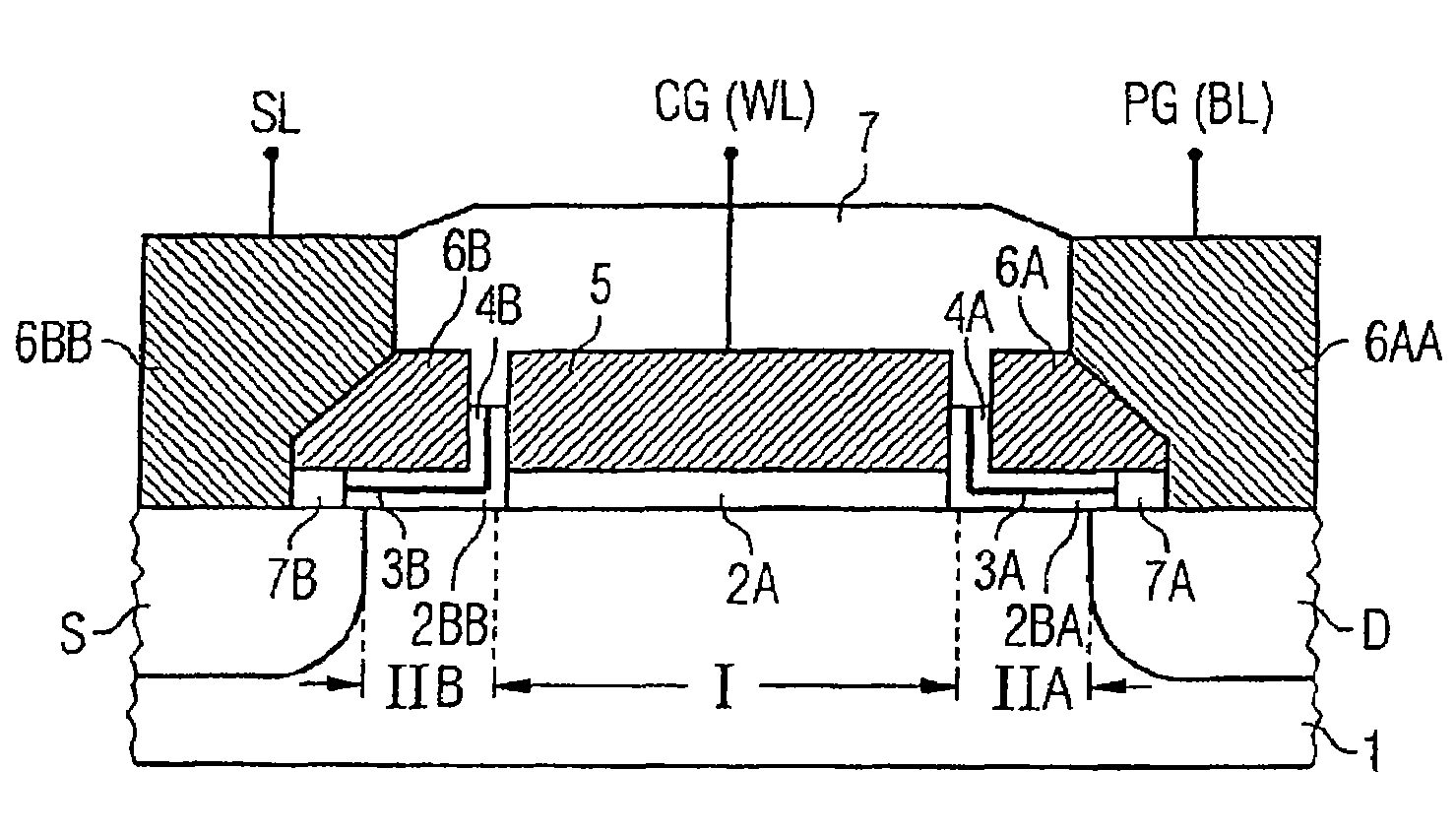
[0037]In the text which follows, the invention will be described by means of a dual-bit split-gate storage element for storing two memory states in a source side and drain side area but, in principle, corresponding nonvolatile semiconductor storage elements for storing only a single state are also conceivable. In particular, it should be pointed out that due to the symmetry of the storage element shown in the figures, the source region and the drain region can be considered as being equivalent and, in consequence, are also correspondingly interchangeable. In particular, this also applies to the source side and drain side layers, where only the respective connection potentials need to be exchanged.

[0038]FIG. 5 shows a simplified sectional view of a dual-bit split-gate storage element according to the invention, identical reference symbols representing identical or corresponding layers and elements as in FIGS. 1 to 4 and a repeated description being omitted in the text which follows.

[...


PUM


Abstract

The invention relates to a nonvolatile semiconductor storage element and an associated production and control method, the storage element includes a semiconductor substrate having a source region, a drain region and an intermediate channel region. On a first portion of the channel region, a control layer is formed and insulated from the channel region by a first insulating layer whereas respective charge storage layers are formed in a second portion of the channel region and are insulated from the channel region by a second insulating layer. On the charge storage layer, a programming layer is formed and insulated from the charge storage layer by a third insulating layer and is electrically connected to a respective source region and drain region via a respective interconnect layer.

Description

TECHNICAL FIELD[0001]The present invention relates to a nonvolatile semiconductor storage element and an associated production and control method and, in particular, to a nonvolatile dual-bit split-gate storage cell in which information is written in by means of charge carrier injection at the source.BACKGROUND[0002]Nonvolatile semiconductor memories which are known, for example, as FLASH memory, EPROM, EEPROM, FPGAs and the like, are becoming more and more successful in many fields such as, e.g. dataprocessing, telecommunications, entertainment, electronics and security technology since they can store data in a very small space over a long period and without using a supply voltage.[0003]In this connection, there is a multiplicity of different storage element types, the present invention relating to, in particular, a so-called split-gate storage cell.[0004]FIG. 1 shows a simplified sectional view of such a conventional split-gate storage element.[0005]According to FIG. 1, a channel ...

Claims


Application Information

Patent Timeline
IPC IPC(8): H01L29/788H01L29/76H01L21/8247G11C16/04H01L21/28H01L21/336H01L27/115H01L29/792
CPCH01L29/7923H01L29/66833H01L21/28282G11C16/0475H01L29/40117
Inventor SCHULER, FRANZTEMPEL, GEORG
Owner INFINEON TECH AG
Why Eureka
Try Eureka