
Charged particle beam apparatus, scanning electron microscope, and sample observation method using the same

a particle beam and electron microscope technology, applied in the field of wafer manufacturing methods, can solve problems such as wrong detection, and achieve the effects of reducing in-plane variation of detection efficiency, reducing deflection color aberration, and reducing chromatic aberration

Inactive Publication Date: 2009-07-07
HITACHI HIGH-TECH CORP
View PDF15 Cites 10 Cited by
  • Summary
  • Abstract
  • Description
  • Claims
  • Application Information

AI Technical Summary

Benefits of technology

The present invention provides a charged particle beam apparatus and a sample observation method that can correct the deflection aberration of the primary electron beam in the indirect detection method of secondary electrons. This is achieved by using a secondary electron conversion unit with a secondary electron conversing electrode and two E×B deflectors to reduce the deflection chromatic aberration and in-plane variation of detection efficiency. The invention can also reduce shading in the secondary electron images caused by dapples of brightness in the surface layer of the sample.

Problems solved by technology

However, the surface of a semiconductor wafer is often covered with an insulator to form a circuit, dapples of brightness in the image (shadings) not attributable to defects often develop on the secondary electron image due to an electrostatic charge of the sample, after the irradiation of primary electron beam.
Such shadings are highly likely to cause wrong detections in the process of detecting defects in the secondary electron images.

Method used


Image

  • Charged particle beam apparatus, scanning electron microscope, and sample observation method using the same
  • Charged particle beam apparatus, scanning electron microscope, and sample observation method using the same
  • Charged particle beam apparatus, scanning electron microscope, and sample observation method using the same

Examples


first embodiment

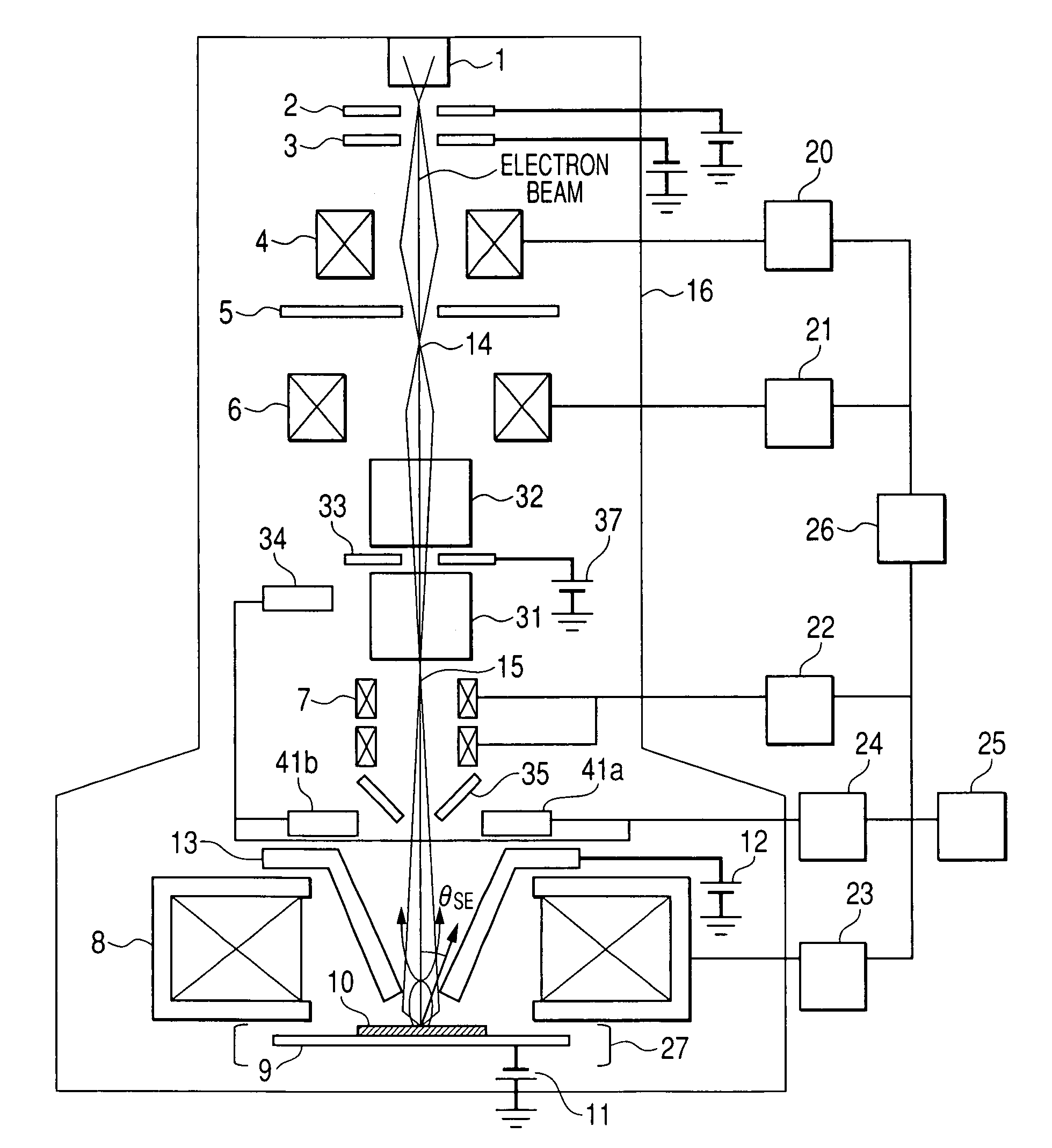
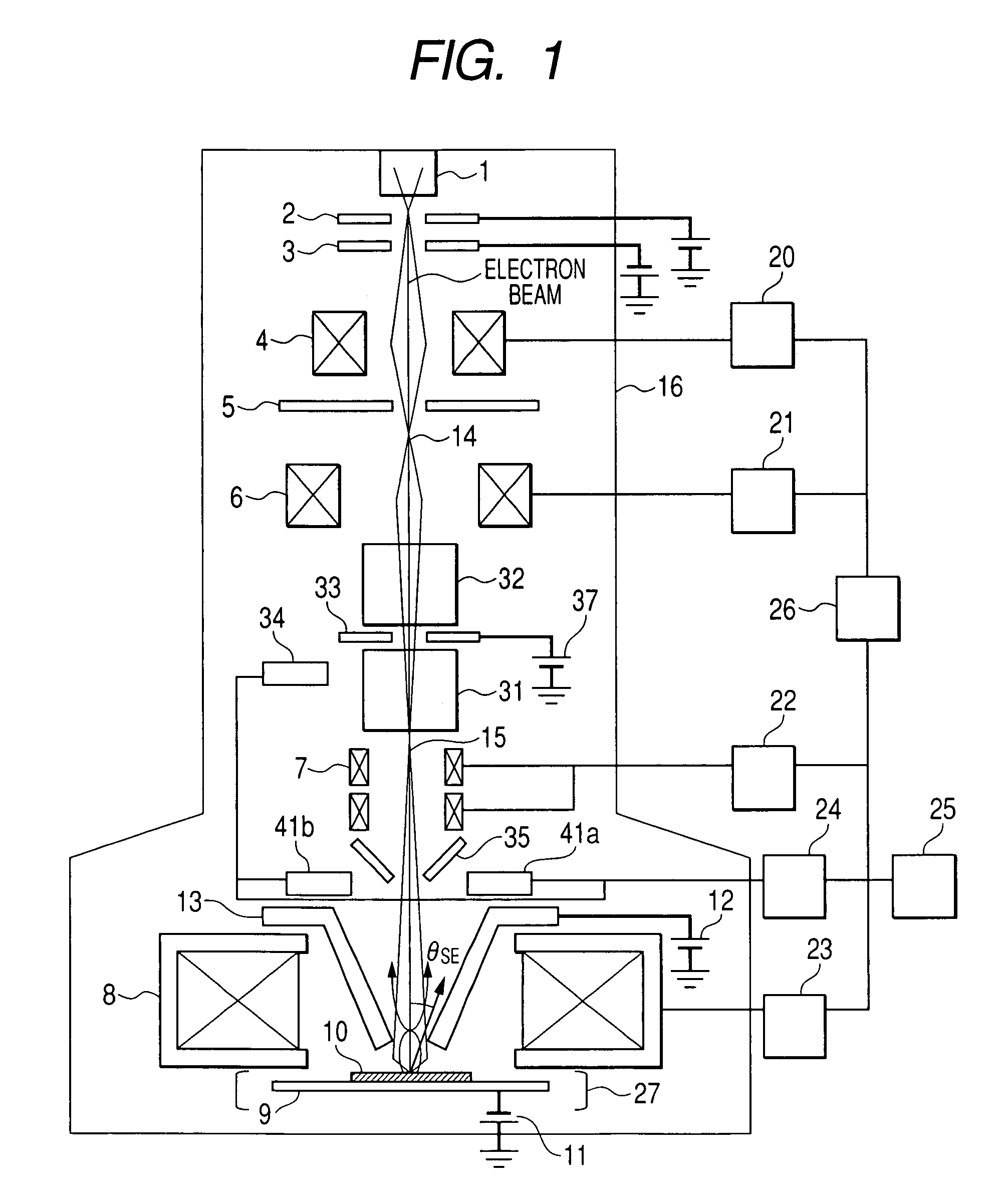
[0029]FIG. 1 shows a review SEM (scanning electron microscope) constituting the first embodiment. The review SEM of this embodiment is an apparatus designed to obtain the image of defects or foreign matters in a semiconductor wafer, to detect fatal defects and classify the detected defects.

[0030]The review SEM is an electron beam applied apparatus carried out by a scanning electron microscope having a semi-in-lens objective lens, and includes roughly speaking an electron optical system, a sample chamber 27, a control unit 26 and an electronic detection system.

[0031]The electronic optical system includes an electronic gun 1, an extraction electrode 2, an acceleration electrode 3, a first condenser lens 4, a second condenser lens 6, an aperture diaphragm 5, a scanning deflector 7, an objective lens 8, and a magnetic electrode 13 above the objective lens. The sample chamber 27 includes a stage 9. The magnetic electrode 13 above the objective lens includes a booster voltage power source...

second embodiment

[0065]FIG. 5 shows a second embodiment. The configuration of this embodiment is a configuration in which the position of the deflector 31 and that of the deflector 32 in the first embodiment are switched. FIG. 5 shows the same configuration as that of the first embodiment except the position of the deflector 31 and the deflector 32. The configuration of the second embodiment is characterized in that the deflector 31 for deflecting the secondary electrons is located closer to the side of the electron source than the deflector 32 for correcting aberration and is connected with the secondary electron conversing electrode 33 through an insulator. The deflector 31 and the deflector 32 are connected through an insulator, and are operated in such a way that their polarity of deflection may be reverse. In the first place, the secondary electrons are deflected by the deflection field created by the deflector 32 for correcting aberration. After passing through the deflection field mentioned a...

third embodiment

[0066]Then, we will describe a third embodiment. While, in the first embodiment, the whole secondary electron conversing electrode was set in a same potential, in this embodiment, a secondary electron conversing electrode 33′ having a structure capable of changing continuously potential is used as the secondary electron conversing electrode. We will describe the secondary electron conversing electrode 33′ of this embodiment with reference to FIG. 6. It is the same as the first embodiment except the structure of the secondary electron conversing electrode. In the first place, a thin metal foil having an equivalent dimension and shape as the surface area of the secondary electron conversing electrode is divided and cut out into n pieces. The direction of cutting is in the parallel direction with the y axis. And the greater the value of n is, the better. The cut out metal foils will be pasted on the surface of the secondary electron conversing electrode in such a way that they may not ...


PUM

PropertyMeasurementUnit
energyaaaaaaaaaa
energyaaaaaaaaaa
voltageaaaaaaaaaa

Abstract

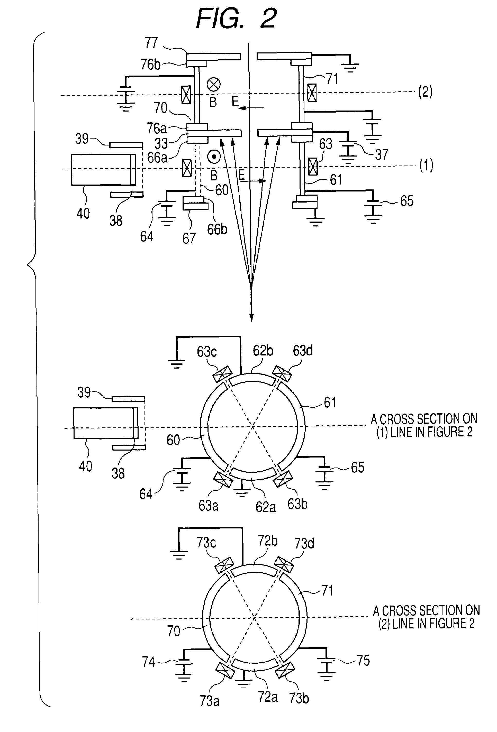
A charged particle beam apparatus for acquiring high-definition and highly contrasted observation images by detecting efficiently secondary signals without increasing aberration of the primary electron beam, detecting defects from observation images and thus increasing the inspection speed and enhancing the sensitivity of inspection. The desired area of the sample is scanned with a primary charged particle beam, and the secondary charged particles generated secondarily from the area by the irradiation of the primary charged particle beam are led to collide with the secondary electron conversing electrode, and then the secondary electrons generated by the first E×B deflector 31 arranged through an insulator on the surface of the secondary electron conversing electrode on the side of the sample is absorbed by the detector. At the same time, the deflection chromatic aberration that had been generated in the primary charged particle beam by the first E×B deflector is reduced by the second E×B deflector arranged on the first E×B deflector, to obtain high-definition and highly contrasted observation images free of shading.

Description

CLAIM OF PRIORITY[0001]The present application claims priority from Japanese application JP 2006-322204 filed on Nov. 29, 2006, the content of which is hereby incorporated by reference into this application.FIELD OF THE INVENTION[0002]The present invention relates to a method for manufacturing a wafer having a circuit pattern, and more particularly to a technique of inspecting a fine pattern using a charged particle beam.BACKGROUND OF THE INVENTION[0003]The scanning electron microscope is an apparatus for accelerating the primary electron discharged from the electron source, converging the same by an objective lens to narrow down the primary electron beam, scanning the sample with the primary electron beams by using a scanning deflector, detecting secondary signals generated from the sample by the irradiation of the primary electron beam and displaying this detected signal intensity as observation image. In order to obtain highly contrasted observation images, an efficient detection...

Claims


Application Information

Patent Timeline
Patent Type & Authority Patents(United States)
IPC IPC(8): G01N23/00G21K7/00
CPCH01J37/153H01J37/244H01J37/28H01J2237/24592H01J2237/2448H01J2237/24485H01J2237/2449H01J2237/057
Inventor SHOJO, TOMOYASUFUKUDA, MUNEYUKISUZUKI, NAOMASA
Owner HITACHI HIGH-TECH CORP
Learn More