
Method of manufacturing nitride semiconductor device including SiC substrate and apparatus for manufacturing nitride semiconductor device

Inactive Publication Date: 2005-03-10
OKI ELECTRIC IND CO LTD
View PDF4 Cites 4 Cited by
  • Summary
  • Abstract
  • Description
  • Claims
  • Application Information

AI Technical Summary

Benefits of technology

[0023] Since the position of the defective part of the SiC substrate of the processed layered product can be specified using the position of the defective part which was specified in the layered product before processing, a chip having the defective part can be eliminated.
[0082] As a result, the position of the defective part of the SiC substrate can be specified automatically and efficiently.

Problems solved by technology

However depositing a nitride semiconductor thin film on the SiC substrate by the abovementioned MOCVD method has the following problems.
First, in the SiC substrate as a crystal substrate, holes called micro-pipes, which penetrate from the front to the back of the substrate, exist as structural defects.
In other words, the structural defects of the SiC substrate causes the generation of defects in the nitride semiconductor thin film on this substrate (this is called defect propagation).
Also in the SiC substrate, various structural defects exist in some cases, other than the abovementioned micro-pipes, such as macro defects (e.g. voids, grain boundaries), dislocations (e.g. spirals, blades, mosaics) and surface defects (surface polishing scratches, surface roughness).
HEMT, which has an SiC substrate with such structural defects, causes operation failures, which drops the reliability as a device.
However the inspection by the system shown in the abovementioned document is not the detection of structural defects but is merely a visual inspection for observing the surface of the device and dimensional errors, and it is impossible to inspect the quality of the device by detecting the abovementioned structural defects.

Method used


Image

  • Method of manufacturing nitride semiconductor device including SiC substrate and apparatus for manufacturing nitride semiconductor device
  • Method of manufacturing nitride semiconductor device including SiC substrate and apparatus for manufacturing nitride semiconductor device
  • Method of manufacturing nitride semiconductor device including SiC substrate and apparatus for manufacturing nitride semiconductor device

Examples


first embodiment

[0103] First Embodiment

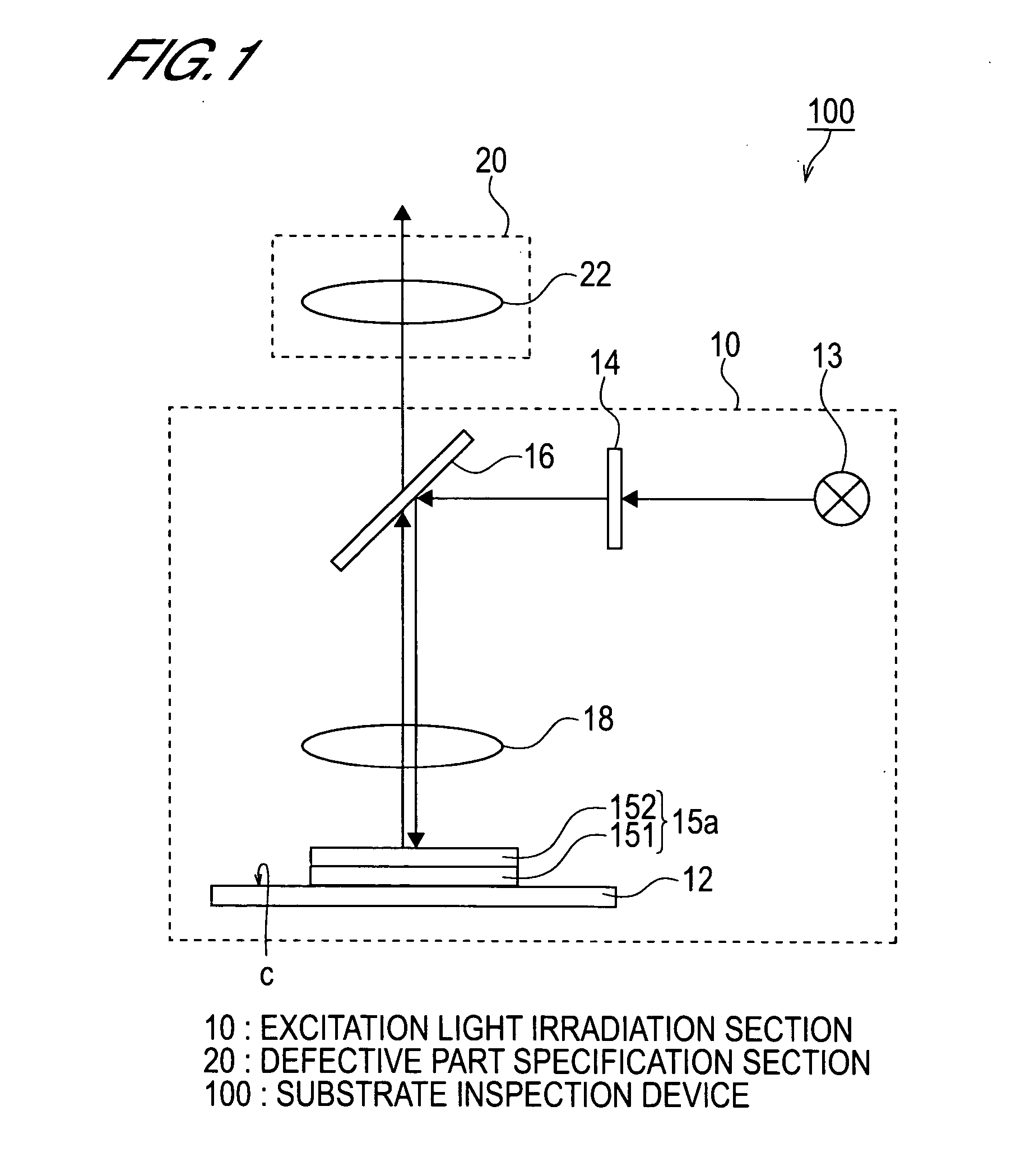
[0104]FIG. 1 is a diagram depicting the configuration of the substrate inspection device 100 of the present embodiment. In the present embodiment, the case when the layered product 15a, where a GaN layer 152 is deposited as a nitride semiconductor thin film on the wafer type silicon carbide (SiC) substrate 151 is used, will be described as an example.

[0105] As FIG. 1 shows, the substrate inspection device 100 of the present embodiment comprises an excitation light irradiation section 10 and a defective part specification section 20. The defective part is an area of the SiC substrate that has a structural defect, and here the area emitting light at the light intensity that is at least a predetermined standard value, which will be described later, will be handled as the defective part.

[0106] The excitation light irradiation section 10 irradiates the excitation light onto the GaN layer 152 as the nitride semiconductor thin film that the layered product 15a has....

second embodiment

[0119] Second Embodiment

[0120] In this embodiment, a mercury lamp, which can irradiate ultraviolet light, is used as the light source of the substrate inspection device, which is a major difference from the first embodiment.

[0121] In this configuration example, a mercury lamp, which can irradiate ultraviolet light, is used rather than the light source described in the first embodiment. In this case, the excitation light is an i-line (wavelength 365 nm) or j-line (wavelength 313 nm).

[0122] In the case of the first embodiment, the entire surface of the sample is brightly lit since visible light is irradiated as the excitation light. Therefore when the defective part of the SiC substrate is observed by the density difference of the luminescence using the naked eye, the density difference of the luminescence, due to blockage by dirt and dust attached to the surface of the sample, may make it difficult to distinguish whether it is a defective part or not.

[0123] If ultraviolet light is...

third embodiment

[0126] Third Embodiment

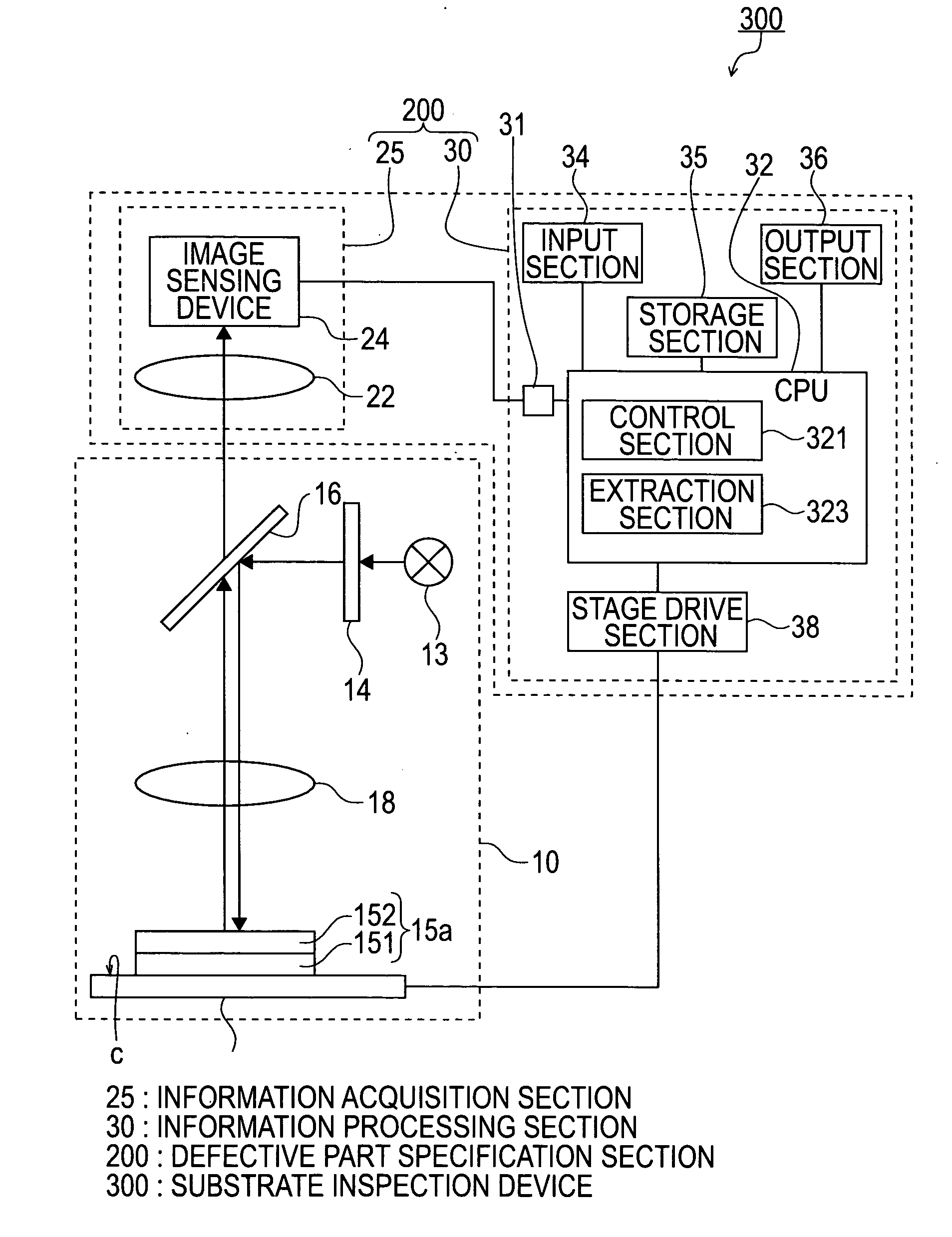
[0127] The substrate inspection device 300 of this embodiment comprises the information acquisition section 25 and the information processing section 30, as the defective part specification section 200, which is a major difference from the first embodiment. In FIG. 3, constitutional elements the same as the constitutional elements described in the first embodiment are denoted with the same reference numerals, and a concrete description thereof will be omitted (this is the same as for each embodiment herein below).

[0128] As FIG. 3 shows, the substrate inspection device 300 of this embodiment comprises the excitation light irradiation section 10 and the defective part specification section 200, just like the first embodiment, but the difference is that this defective part specification section 200 further comprises the information acquisition section 25 and the information processing section 30.

[0129] In the information acquisition section 25, the surface area...


PUM


Abstract

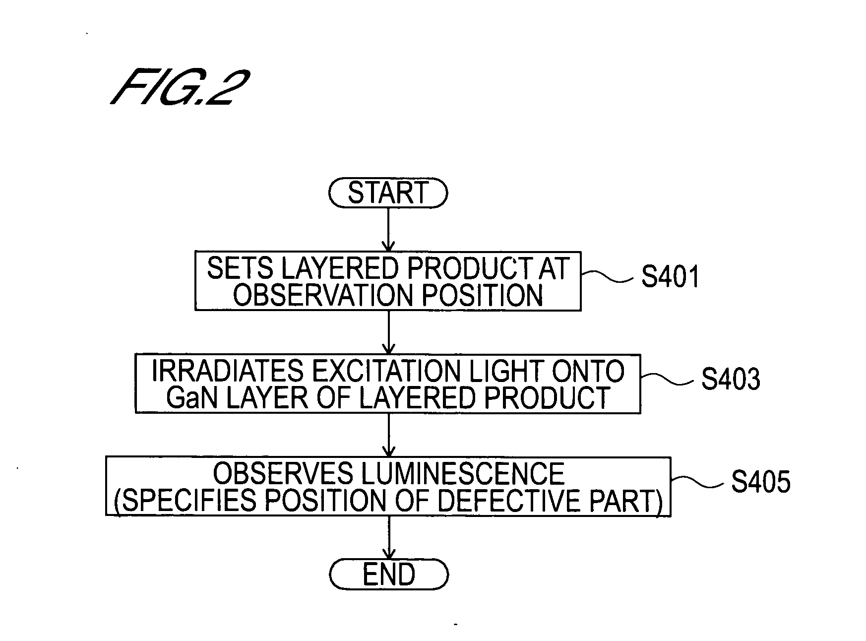
Excitation light is irradiated onto a GaN layer on a silicon carbide substrate constituting a layered product that is set on a stage. Then light is emitted from a defective part caused by a structural defect of the silicon carbide substrate out of the GaN layer. By using this light luminescence phenomena, a position of a defective part of the silicon carbide substrate can be detected.

Description

BACKGROUND OF THE INVENTION [0001] 1. Field of the Invention [0002] The present invention relates to a substrate inspection method and substrate inspection device that are suitable for use in a silicon carbide (SiC) substrate constituting a nitride semiconductor device, and a method of manufacturing the nitride semiconductor device and an apparatus for manufacturing for the nitride semiconductor device using the substrate inspection method and the substrate inspection device. [0003] 2. Description of Related Art [0004] At the moment, research on nitride semiconductors is actively progressing in the fields of optical devices and electronic devices because of advantages in physical characteristics. [0005] In particular, in the electronic device field, the development of high electron mobility transistors (hereafter called “HEMT”) using nitride semiconductors is now in progress. [0006] In the case of nitride semiconductor crystals, growing bulk single crystals is difficult because vapo...

Claims


Application Information

Patent Timeline
IPC IPC(8): G01N21/88H01L21/66H01L33/32H01L33/34H01S5/00
CPCH01L22/22H01L2924/0002H01L2924/00
Inventor TODA, FUMIHIKO
Owner OKI ELECTRIC IND CO LTD
Learn More