

Method of manufacturing nitride semiconductor device including SiC substrate and apparatus for manufacturing nitride semiconductor device
a technology of nitride semiconductor and semiconductor device, which is applied in the direction of semiconductor/solid-state device testing/measurement, instruments, semiconductor lasers, etc., can solve the problems of nitride semiconductor thin film generation, various structural defects, surface roughness,
- Summary
- Abstract
- Description
- Claims
- Application Information
AI Technical Summary
Benefits of technology
Problems solved by technology
Method used
Image

Examples
first embodiment
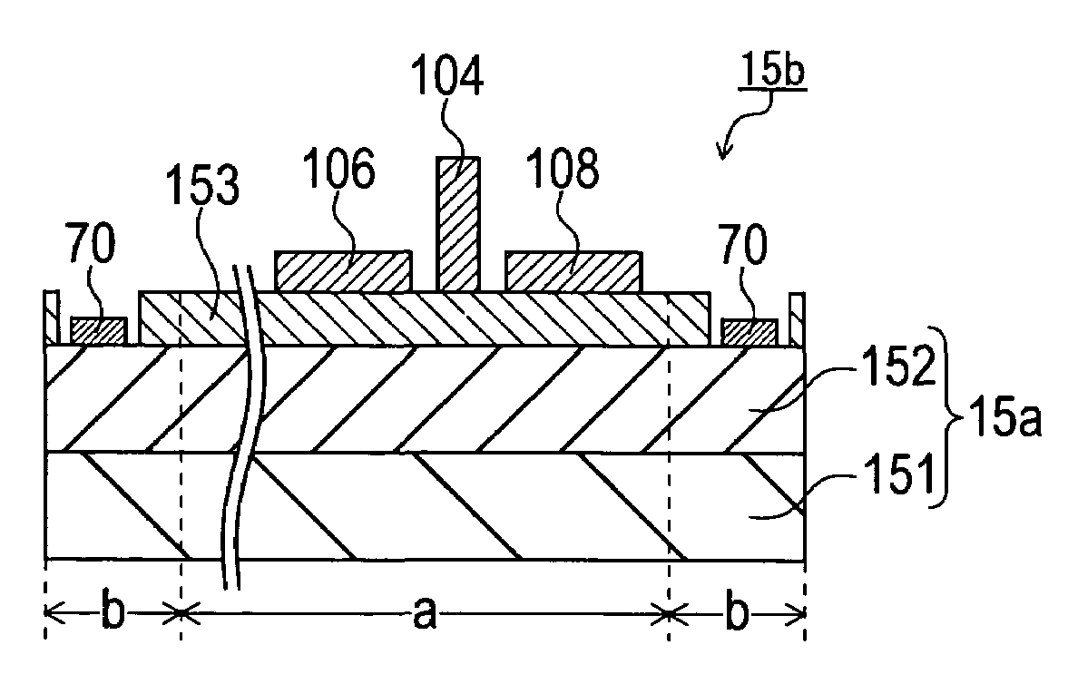
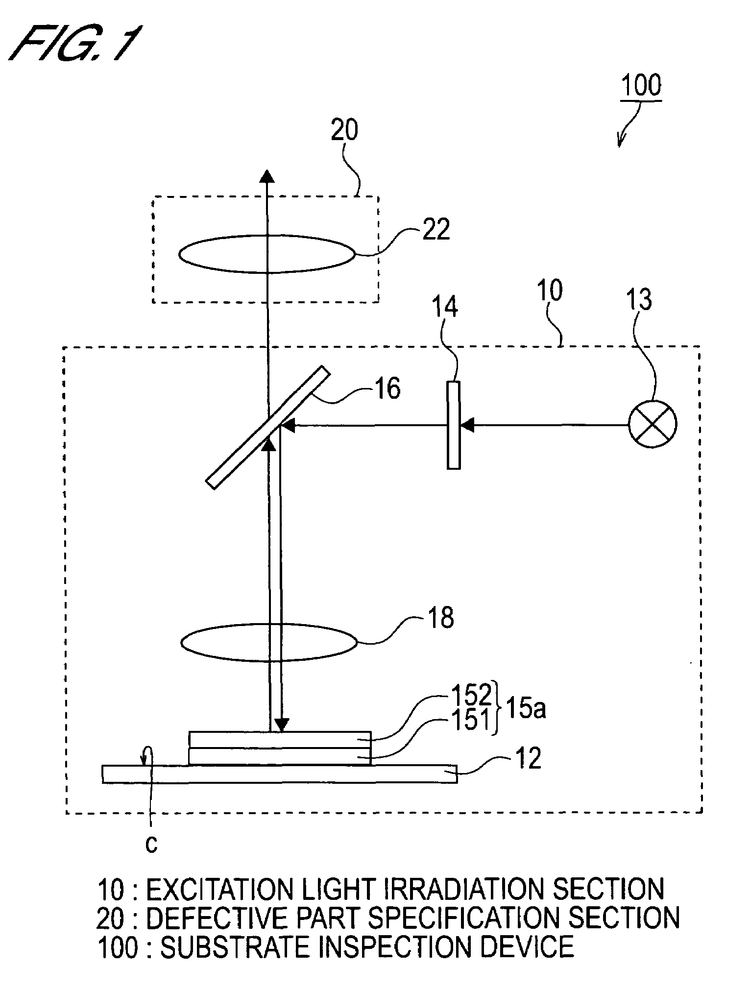
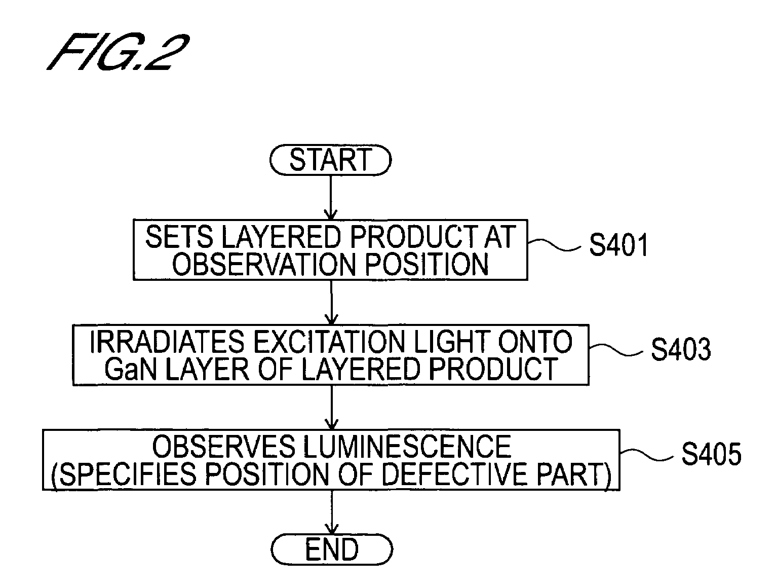
[0103]FIG. 1 is a diagram depicting the configuration of the substrate inspection device 100 of the present embodiment. In the present embodiment, the case when the layered product 15a, where a GaN layer 152 is deposited as a nitride semiconductor thin film on the wafer type silicon carbide (SiC) substrate 151 is used, will be described as an example.
[0104]As FIG. 1 shows, the substrate inspection device 100 of the present embodiment comprises an excitation light irradiation section 10 and a defective part specification section 20. The defective part is an area of the SiC substrate that has a structural defect, and here the area emitting light at the light intensity that is at least a predetermined standard value, which will be described later, will be handled as the defective part.
[0105]The excitation light irradiation section 10 irradiates the excitation light onto the GaN layer 152 as the nitride semiconductor thin film that the layered product 15a has.
[0106]Here the excitation l...
second embodiment
[0118]In this embodiment, a mercury lamp, which can irradiate ultraviolet light, is used as the light source of the substrate inspection device, which is a major difference from the first embodiment.
[0119]In this configuration example, a mercury lamp, which can irradiate ultraviolet light, is used rather than the light source described in the first embodiment. In this case, the excitation light is an i-line (wavelength 365 nm) or j-line (wavelength 313 nm).
[0120]In the case of the first embodiment, the entire surface of the sample is brightly lit since visible light is irradiated as the excitation light. Therefore when the defective part of the SiC substrate is observed by the density difference of the luminescence using the naked eye, the density difference of the luminescence, due to blockage by dirt and dust attached to the surface of the sample, may make it difficult to distinguish whether it is a defective part or not.
[0121]If ultraviolet light is irradiated as the excitation l...
third embodiment
[0124]The substrate inspection device 300 of this embodiment comprises the information acquisition section 25 and the information processing section 30, as the defective part specification section 200, which is a major difference from the first embodiment. In FIG. 3, constitutional elements the same as the constitutional elements described in the first embodiment are denoted with the same reference numerals, and a concrete description thereof will be omitted (this is the same as for each embodiment herein below).
[0125]As FIG. 3 shows, the substrate inspection device 300 of this embodiment comprises the excitation light irradiation section 10 and the defective part specification section 200, just like the first embodiment, but the difference is that this defective part specification section 200 further comprises the information acquisition section 25 and the information processing section 30.
[0126]In the information acquisition section 25, the surface area of the inspection target Si...
PUM
| Property | Measurement | Unit |
|---|---|---|
| wavelength | aaaaa | aaaaa |
| incident angle | aaaaa | aaaaa |
| incident angle | aaaaa | aaaaa |
Abstract
Description
Claims
Application Information