Thin film forming method and system

a thin film and protective layer technology, applied in the field of thin film forming methods and systems, can solve the problems of reducing the thickness of the overcoat, affecting the quality of the overcoat,

Active Publication Date: 2009-07-14
SAE MEGNETICS H K
View PDF3 Cites 2 Cited by
  • Summary
  • Abstract
  • Description
  • Claims
  • Application Information

AI Technical Summary

Benefits of technology

[0012]By depositing a forming material on an object while etching the forming material, the method and system not only improves the adhesion and coverage properties of the film formed on the object, but also decrease the deposition rate significantly and accordingly extend the deposition time, then the uniformity of the protective film formed on one-batch objects can be improved significantly. A lower deposition rate also minimize the influence of opening and closing the shutter on the uniformity of the protective films. In addition, the method also overcome the current thickness limitation (i.e. equal or more than 3 nm) of the protective film with superior reliability of the conventional film forming method.

Problems solved by technology

Some of these metal materials are very prone to be corroded or damaged.
However, these methods have arrived at a stage where their limitation to scale down a thickness of overcoat is clearly visible, for the following reasons.
These defects show up in the course of manufacturing, application or reliability tests for magnetic devices.
Another problem associated with these methods is that the high deposition rate results in a very short time to form an ultra thin overcoat (i.e. equal or less than 3 nm), and this makes the overcoats formed on the magnetic devices in one batch non-uniform.
During the course of opening or closing the shutter, there are still some ion beams bombarding the magnetic devices, which also contributes to the non-uniformity of the overcoats formed on one batch magnetic devices.

Method used


Image

  • Thin film forming method and system
  • Thin film forming method and system
  • Thin film forming method and system

Examples


Embodiment Construction

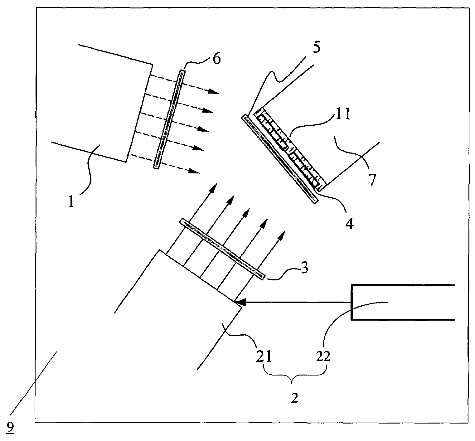
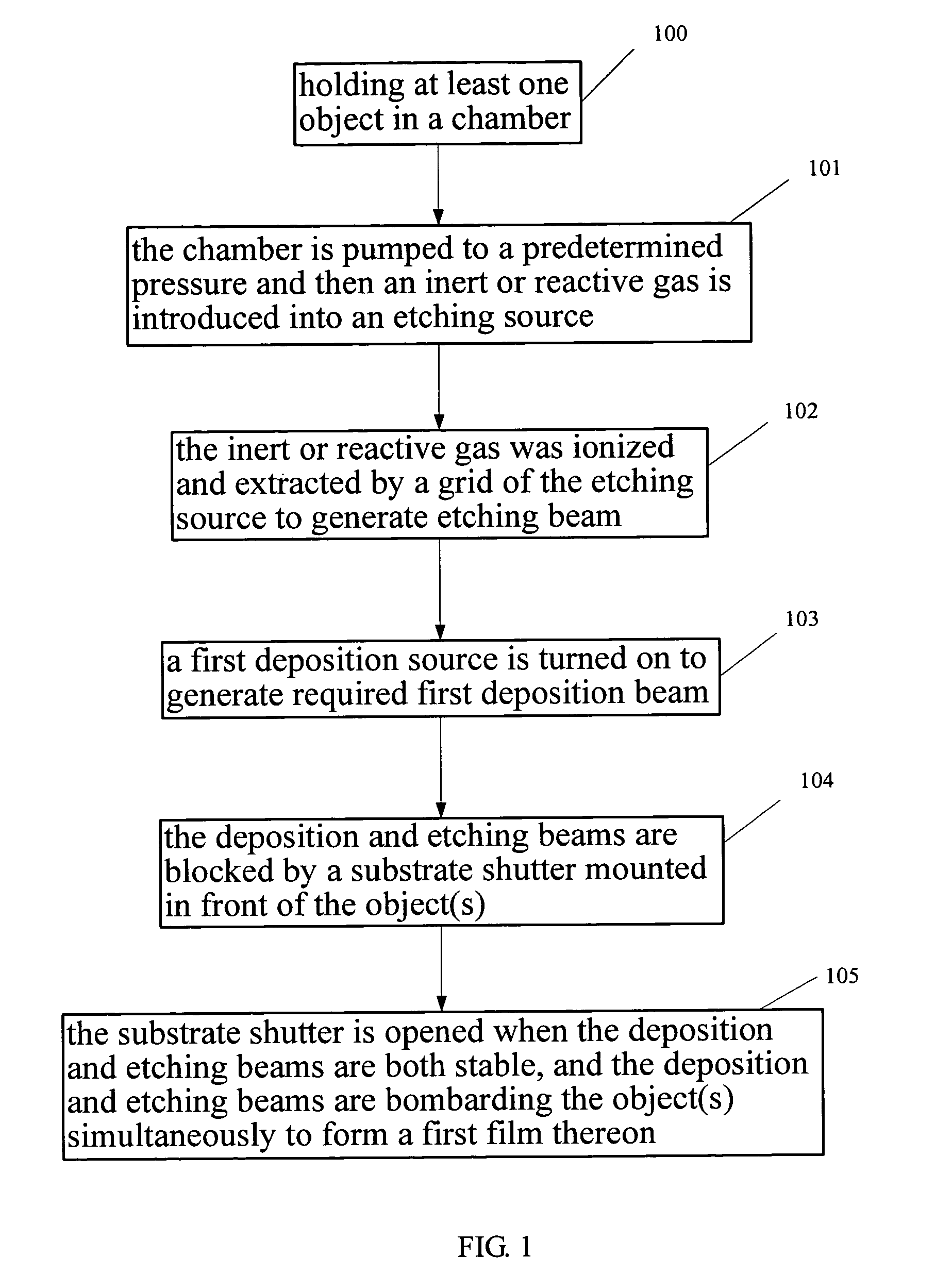
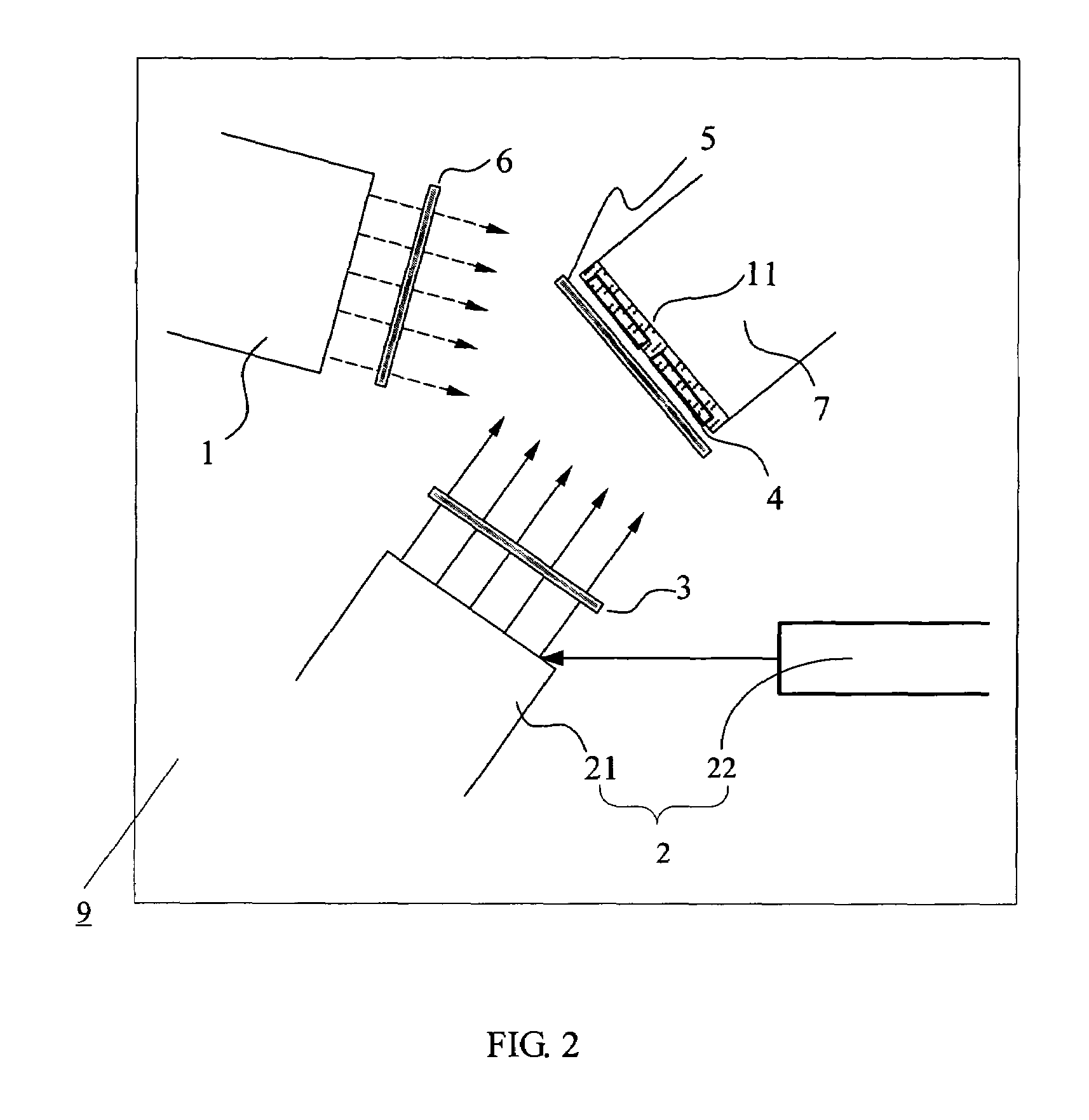
[0022]A thin film forming method of the present invention comprises the steps of: (1) holding at least one object in a chamber; (2) depositing a film-forming material on the object; and (3) etching the film-forming material while depositing is conducted. In the present invention, the depositing and etching are conducted simultaneously. The depositing step comprises placing a target for forming a film and irradiating ion beam to bombard the target. The etching step comprises the steps of: (1) providing an atmosphere of inert or reactive gas at a predetermined pressure in a chamber; and (2) ionizing the atmosphere to generate etching beam to bombard the object.

[0023]Referring now to the drawings in detail, FIG. 1 shows a flow chart of a thin film forming method according to an embodiment of the present invention. The method comprises the following steps: (1) holding at least one object in a chamber (Step 100); (2) the chamber is pumped to a predetermined pressure and then an inert or ...


PUM

PropertyMeasurementUnit
pressureaaaaaaaaaa
ion energyaaaaaaaaaa
thicknessaaaaaaaaaa

Abstract

A thin-film forming method, which includes the steps of: (1) holding at least one object in a chamber; (2) depositing a film-forming material on the object; (3) etching the forming material while depositing is conducted. In the present invention, the depositing and etching are controlled to simultaneously conduct. The invention also disclose a system for performing the method.

Description

FIELD OF THE INVENTION[0001]The present invention is related to a method and system of forming a thin film layer, a protective layer, and a friction-free layer, and more particularly to a method and system for forming a protective layer over a magnetic device thereon.BACKGROUND OF THE INVENTION[0002]At present, magnetic devices, such as magnetic read / write heads, magnetic disks, are being widely used in data storage industry. Referring to FIG. 4, a typical magnetic read / write head, such as magneto-resistance (MR) head, generally comprises a substrate 34, shields 33, a MR element 35, a coil 32 and a yoke 31. Referring to FIG. 6, a typical magnetic disk has a substrate 10, a buffer layer 20, and a magnetic layer 30. Both above magnetic devices have some important elements, such as shield 33, MR element 35, yoke 31, magnetic layer 30, which are made of functional materials, and most of the functional materials are kinds of metal, i.e. Ni, Fe, Mn, Pt, Au, Co, Ti, Cu. Some of these metal...

Claims


Application Information

Patent Timeline
Patent Type & Authority Patents(United States)
IPC IPC(8): B44C1/22C23C16/00C23F1/00
CPCC23C14/022C23C14/221C23F4/00G11B5/8408G11B5/3106G11B5/255G11B5/3163
Inventor FANG, HONGXINMA, HONGTAOZHANG, BAIQINGCHEN, BAOHUACHOUDHURY, SOMEN
Owner SAE MEGNETICS H K
Why Eureka
Try Eureka