Low loss electrical delay line

a delay line and low loss technology, applied in the direction of waveguides, semiconductor devices, semiconductor/solid-state device details, etc., can solve the problems of time further increasing the insertion loss, the transistor fabrication process (mmic) is expensive and requires high resolution, and the inability to provide all the desired attributes, etc., to achieve simplified delay line solution, reduce the dielectric loss, and simplify the effect of delay lin

Active Publication Date: 2009-07-14
BANPIL PHOTONICS
View PDF4 Cites 21 Cited by
  • Summary
  • Abstract
  • Description
  • Claims
  • Application Information

AI Technical Summary

Benefits of technology

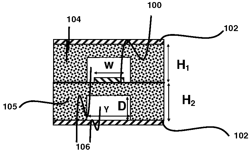
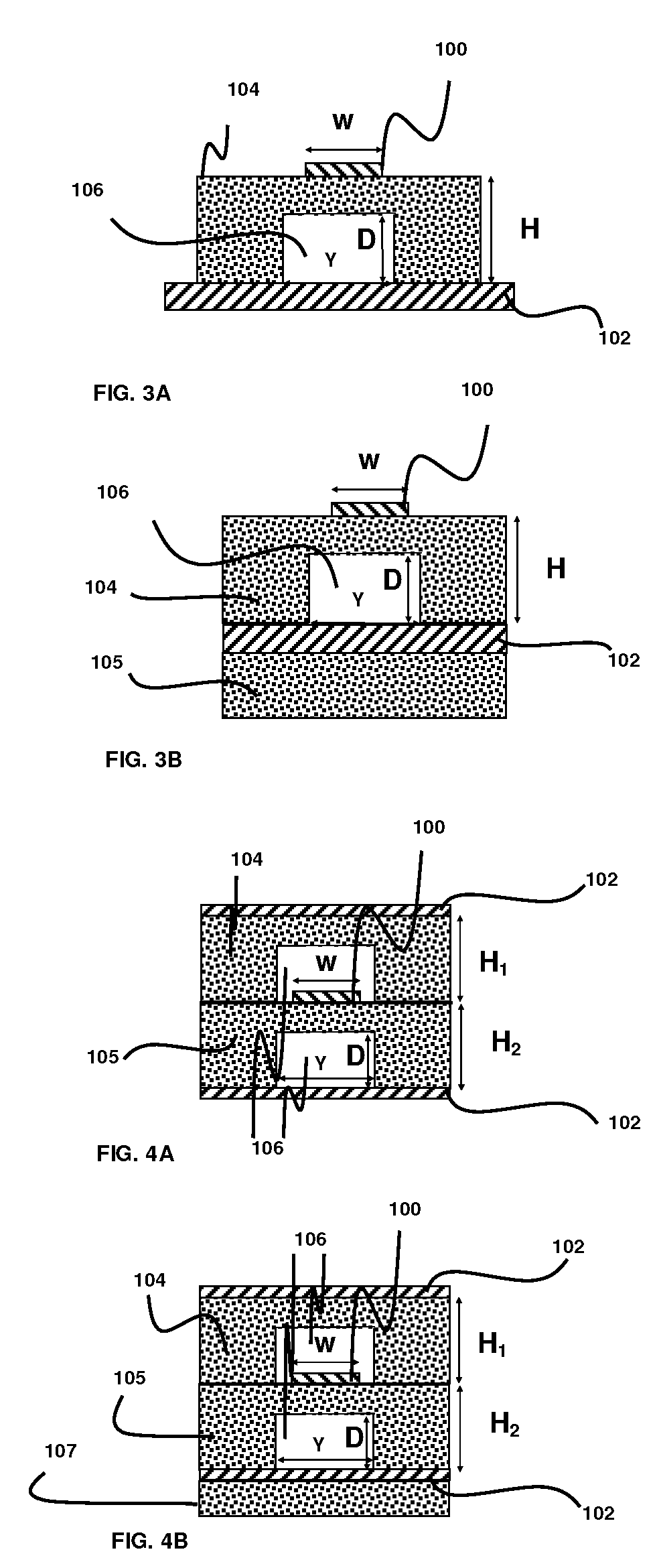
[0010]The invention is an implementation of low loss delay lines in both static and variable configurations. This low loss is achieved by creating a trench or backside slot, made of either an air gap or a material with a lower value dielectric loss / constant than the core dielectric material, within the core dielectric material, under the signal line in order to reduce the effective loss-tangent and effective dielectric constant. This technique results in better performance characteristics than the traditional configuration, which is described within. Other peripheral benefits can be achieved by choosing a dielectric system that has cooling effects or the ability to be controlled and / or varied during operation. Using coolant (gas, liquid etc.) in the trench helps to reduce the heat induced due to the absorption of the signal.
[0012]The invention is a novel delay line technology that will decrease the dielectric loss such that a signal will be transmitted at a much higher frequency. This delay line is passive device. For example, if this high performance passive delay line is used with standard PCB material e.g. FR4 (Trade Name), the estimated loss at 20 GHz at the end of 12 inches is only 2 dB for 70% of trench height with respect to the total height of the substrate; whereas, a 12 inch long state-of-art delay line in standard FR4 based PCB at 20 GHz will have more tha 9 dB of signal loss. This low loss allows standard single ended signaling without equalization or clock and data recovery, hence providing a simplified delay line solution. This delay line can be greatly simplified for microwave delay lines and can be of help when designing tunable delay lines utilizing low-cost FR4 PCB material. Alternatively, this delay line can be also fabricated monolithically on the semiconductor substrate and integrated with other active devices to increase the functionality and also make variable delay line incorporating with other devices such as switches.

Problems solved by technology

State-of-art delay lines are based on active device technologies such as Field-Effect Transistor (FET) and P-I-N diode; however, these are not capable of providing all the desired attributes mentioned earlier because the transistor fabrication process (MMIC) is costly and requires high resolution.
The primary drawbacks concerning this type of delay line are: the insertion loss is dominated by the dielectric materials and a longer delay time further increases the insertion loss.
However, under current technologies the cost of the low loss tangent dielectrics is sufficiently high to limit their usage to high-end systems.
As this structure is made of diodes and not suitable for dealing with the high input of signal,

Method used


Image

  • Low loss electrical delay line
  • Low loss electrical delay line
  • Low loss electrical delay line

Examples


Embodiment Construction

[0028]In the following detailed description of the preferred embodiments, reference is made to the appended drawings which form a part hereof, and within which are shown, by way of illustration, specific embodiments by which the invention may be practiced. It is to be understood that other embodiments may be utilized and structural changes may be made without departing from the spirit and scope of the invention. The following detailed description is, therefore, not to be taken in a limiting sense, and the scope of the present inventions is defined only by the appended claims.

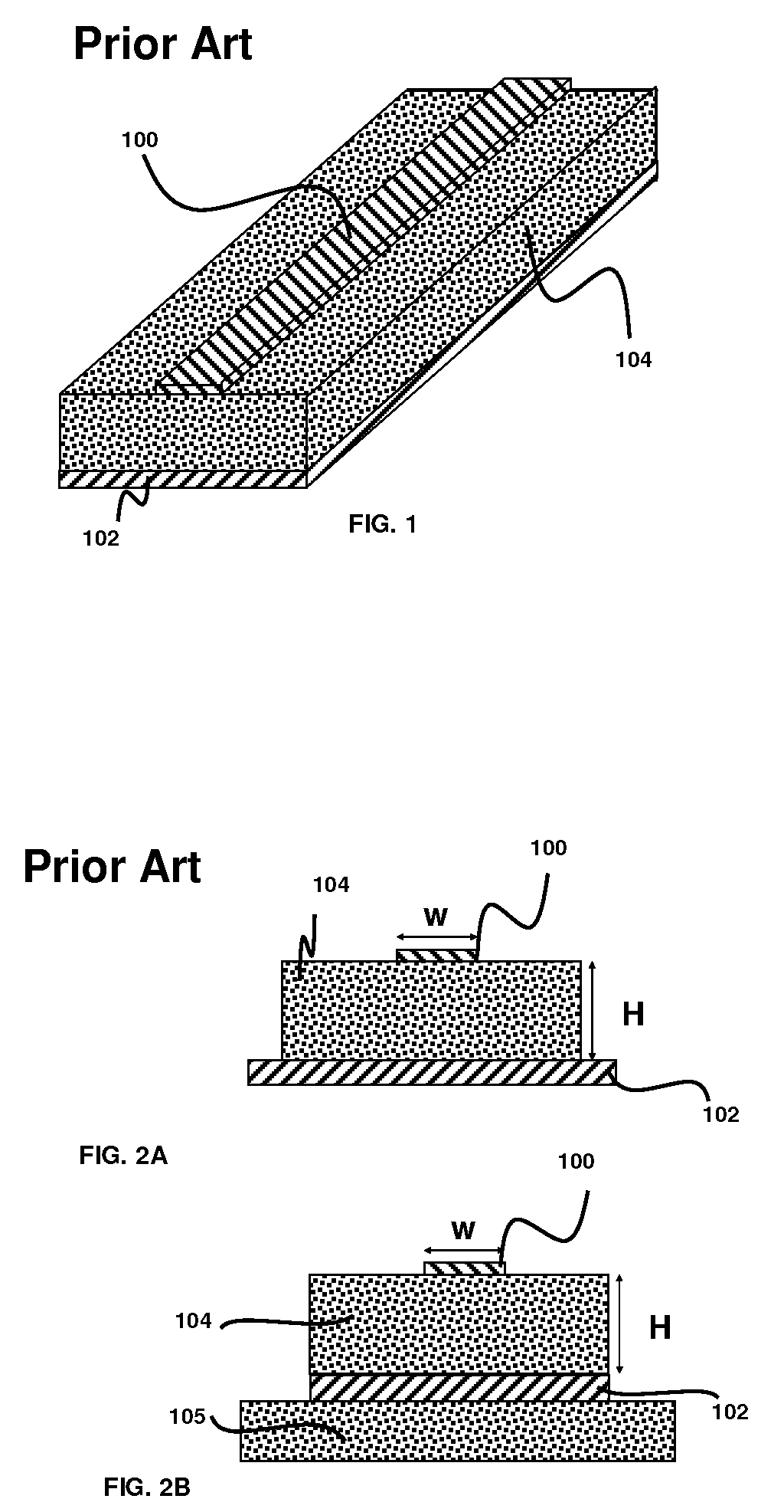
[0029]A single delay line can be as simple as a straight line such as the line shown in FIG. 1, or more complex, including many bends as shown in FIG. 8A-8D. Multiple delay lines can be chained together as shown in FIG. 8E to create a controlled, variable delay line system at the cost of whatever loss is introduced by the switches.

[0030]The structure of each delay line can vary quite significantly. These varianc...


PUM


Abstract

A delay line system able to reduce the microwave loss by reducing the effective dielectric loss and dielectric constant of the system including a signal line, dielectric system with opened trench or slot filled up with the air or lower dielectric loss material, a ground plane, and a system of switches if the line is to be variable. The delay line proposed in this invention could be made of any type of signal line configuration, for example: micro-strip line, strip line, or coplanar line. The signal line can also be made as single ended or differential pairs of any configurations. The delay line systems based on the fundamental techniques provided in this invention can be used for on-chip devices where the delay line is laid on the oxide or dielectric material, or in a traditional PCB implementation such as FR4.

Description

CROSS REFERENCE TO RELATED APPLICATIONS[0001]This patent application is related to U.S. patent application Ser. Nos. 10 / 793,576, and 10 / 793,363 filed concurrently herewith and entitled “High speed interconnects and manufacturing” which is hereby incorporated by reference herein in its entirety.FIELD OF THE INVENTION[0002]The present invention relates to achieving low loss delay lines (mentioned as also “Phase-Shifter”) by creating a trench, made of either an air gap or a material with a lower value dielectric than the core dielectric material, within the core dielectric material. It is used best in systems which require a shift in phase or a signal delay.BACKGROUND OF THE INVENTION[0003]Delay-Lines with attributes of low insertion loss, low cost, high power signal handling, and which are variable are desired for numerous microwave applications. Especially, in modern high frequency radar and communication systems, the antenna pattern must be moved at very rapid rates and this is norm...

Claims


Application Information

Patent Timeline
Patent Type & Authority Patents(United States)
IPC IPC(8): H01P1/18H01P3/08H01P9/00
CPCH01L23/66H01P3/003H01P3/08H01P9/00H01L2223/6627H01L2924/09701H01L2924/12044H01L2924/19032H01L2924/3011H01L2924/0002H01L2924/00
Inventor DUTTA, ACHYUT KUMAR
Owner BANPIL PHOTONICS
Why Eureka
Try Eureka