Matrix image recorder with image sensor and a plurality of row conductors

a matrix image and sensor technology, applied in the field of matrix image sensors, can solve the problems of reducing the sensitivity of a given pixel size, increasing the pixel size, and not allowing easy separation between images, so as to achieve good compromise and improve the pixel structure

Inactive Publication Date: 2009-07-14
ATMEL GRENOBLE
View PDF22 Cites 4 Cited by
  • Summary
  • Abstract
  • Description
  • Claims
  • Application Information

AI Technical Summary

Benefits of technology

[0005]The object of the invention is to provide an improved pixel structure for a sensor in CMOS technology, allowing a good compromise between these various parameters (sensor size, resolution, sensitivity), while still allowing exposure time control and simultaneous exposure of all the pixels of the sensor before the image captured by the set of pixels is read.
[0014]The structure of each pixel of the matrix is therefore a structure comprising five transfer gates and one photosensitive region, thereby constituting a relatively complex circuit at the intersection between each row and each column, but the configuration according to the invention is such that the pixels are connected to the peripheral drivers only via four conductors (apart from the supply and ground) which are the following: two row conductors (one for selection and one for resetting each new acquisition); one column conductor for reading the image acquired; and a conductor common to all the pixels for controlling the exposure time. This number is particularly small taking into account the complexity of the operation of an image sensor in CMOS technology, and the production constraints may be minimized.

Problems solved by technology

However, it has the drawback of not allowing easy separation between acquisition of an image and reading of this image.
As a result, there is reduced sensitivity for a given pixel size.
Alternatively, at a given sensitivity the result is an increased pixel size and therefore an increase in the size of the chip and of the associated optical objectives, which is expensive, or else the result is a reduction in the number of pixels and therefore in the resolution of the sensor if the size of the chip is maintained.

Method used


Image

  • Matrix image recorder with image sensor and a plurality of row conductors
  • Matrix image recorder with image sensor and a plurality of row conductors
  • Matrix image recorder with image sensor and a plurality of row conductors

Examples


Embodiment Construction

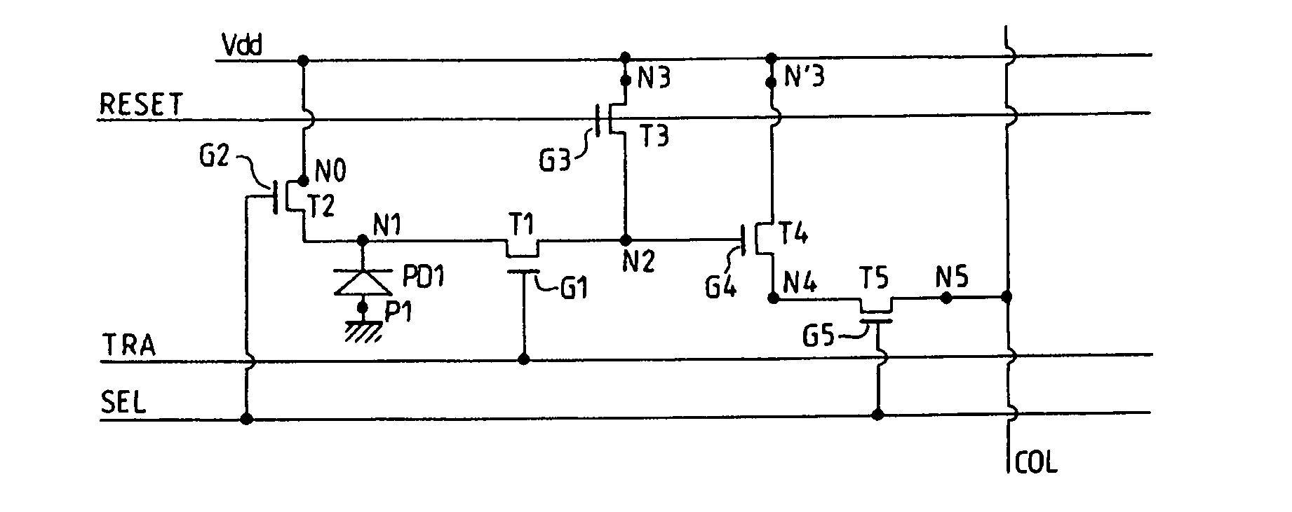
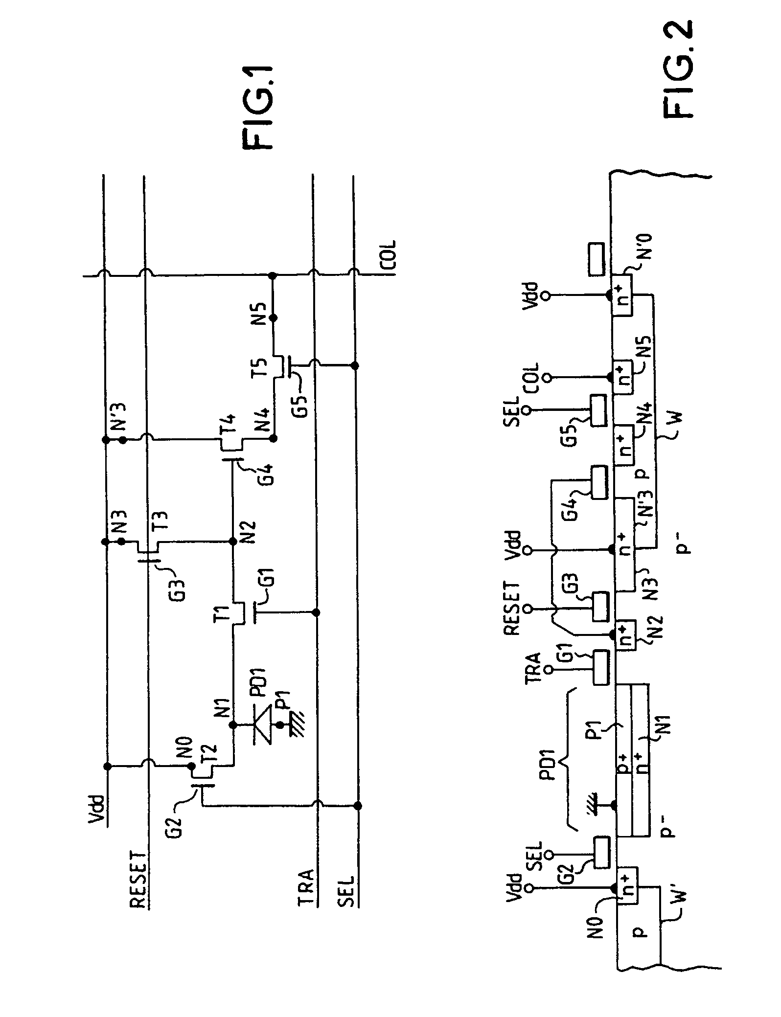
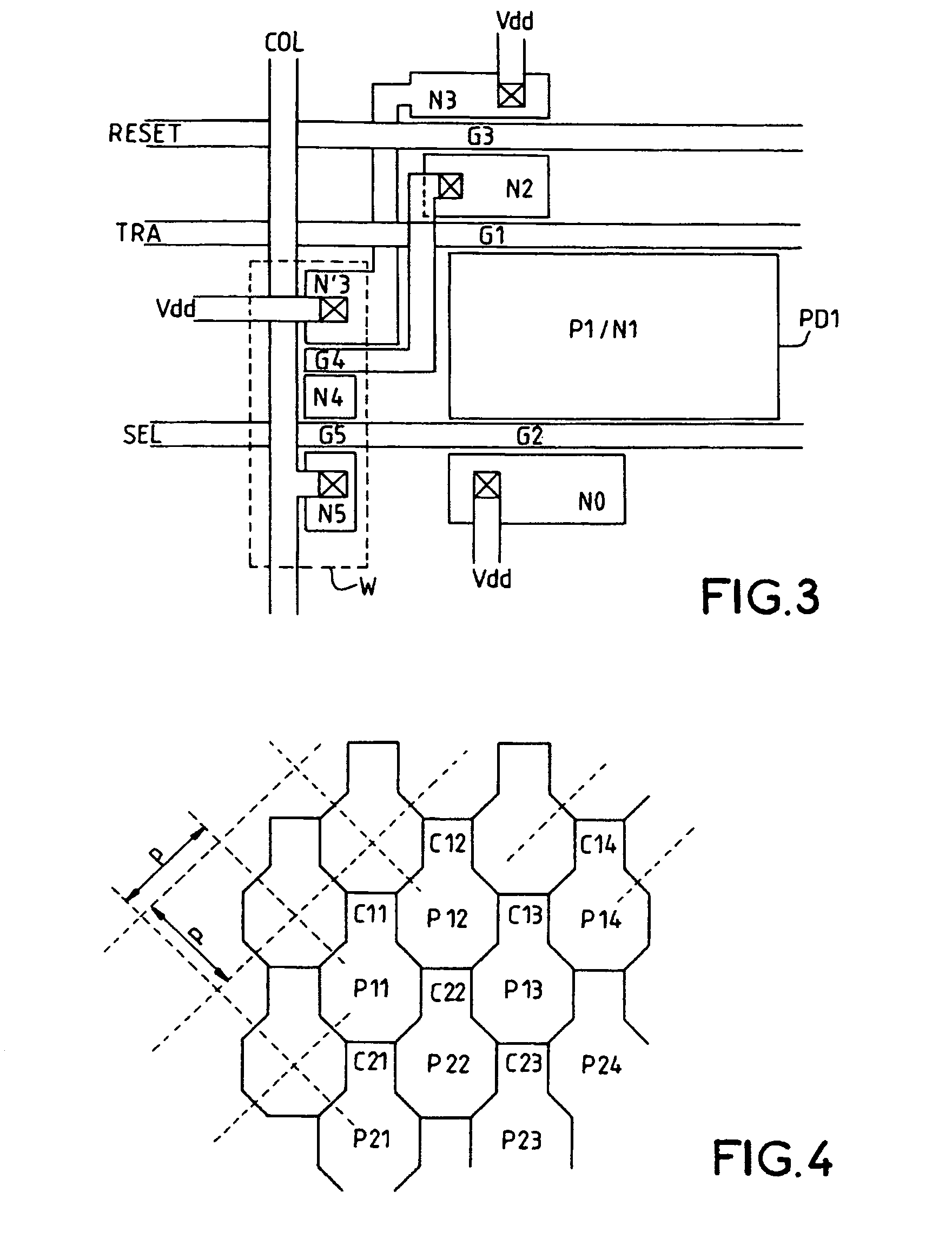
[0027]The matrix image sensor is formed on a semiconductor substrate of p-type conductivity, into which n-type or p-type impurities are locally diffused so as to form p-type regions and n-type regions of variable doping levels. The symbol n+ or p+ will be used to denote n-type or p-type regions that are quite highly doped, and therefore quite highly conducting. The symbol p− will be used to denote lightly doped p-type substrate regions. The bulk of the substrate in which the sensor is formed is of the p−-type.

[0028]The pixel shown in FIGS. 1 and 2 comprises a photosensitive element which in this example is a photosensitive diode formed by the junction between a p+-type region P1 and an n+-type region N1. Preferably, the region P1 is formed on the surface of the substrate and is grounded (at zero supply voltage), the p−-type substrate also being grounded via a p+-type diffusion (not shown). The region N1 is located here entirely below the region P1. The photosensitive region will be ...


PUM


Abstract

The invention relates to matrix image sensors intended in particular for digital photography. The invention provides a driver in each pixel that allows exposure control common to the entire matrix. The driver comprises five transistors, a photodiode and, apart from a supply conductor and a ground, four control conductors, these being an exposure control conductor common to all the pixels of the matrix; a row selection conductor common to all the pixels of any one row; a reset conductor common to all the pixels of any one row; and a column conductor for collecting the signal read on the pixels during row-by-row reading of the charges photogenerated in the pixels of the matrix.

Description

FIELD OF THE INVENTION[0001]The invention relates to matrix image sensors intended in particular for digital photography.BACKGROUND OF THE INVENTION[0002]One conventional technology uses CCD (charge coupled device) sensors, but it is apparent that a CMOS technology could also be used, this having the advantage of allowing both the actual image sensor, that is to say a matrix of photosensitive elements, and complex electronic image processing circuits to be produced on the same silicon integrated circuit chip. This CMOS technology also has the advantage of consuming less energy. However, it has the drawback of not allowing easy separation between acquisition of an image and reading of this image.[0003]Typically, it would be desirable overall to acquire the entire image over an exposure time which not only is the same for all the picture elements (or pixels) but which starts at the same instant for all the elements and terminates at the same instant, before passing to an operation to ...

Claims


Application Information

Patent Timeline
Patent Type & Authority Patents(United States)
IPC IPC(8): H04N3/14H04N5/335H01L27/146H04N5/353H04N5/3745
CPCH01L27/14603H04N5/3745H04N5/353H04N25/53H04N25/77
Inventor BRISSOT, LOUIS
Owner ATMEL GRENOBLE
Why Eureka
Try Eureka