Controlled fabrication of gaps in electrically conducting structures
a technology of electrical conductivity and fabrication, applied in the direction of instruments, suspensions and porous materials analysis, vacuum evaporation coating, etc., can solve the problem of inability to control on a time scale commensurate with the time scale, the gap between nanoelectrodes is not practicable or economical, and the proposed techniques often cannot form the requisite nano-scale features reproducibly or predictably, etc. problem, to achieve the effect of precision and repeatability
- Summary
- Abstract
- Description
- Claims
- Application Information
AI Technical Summary
Benefits of technology
Problems solved by technology
Method used
Image
Examples
example 1
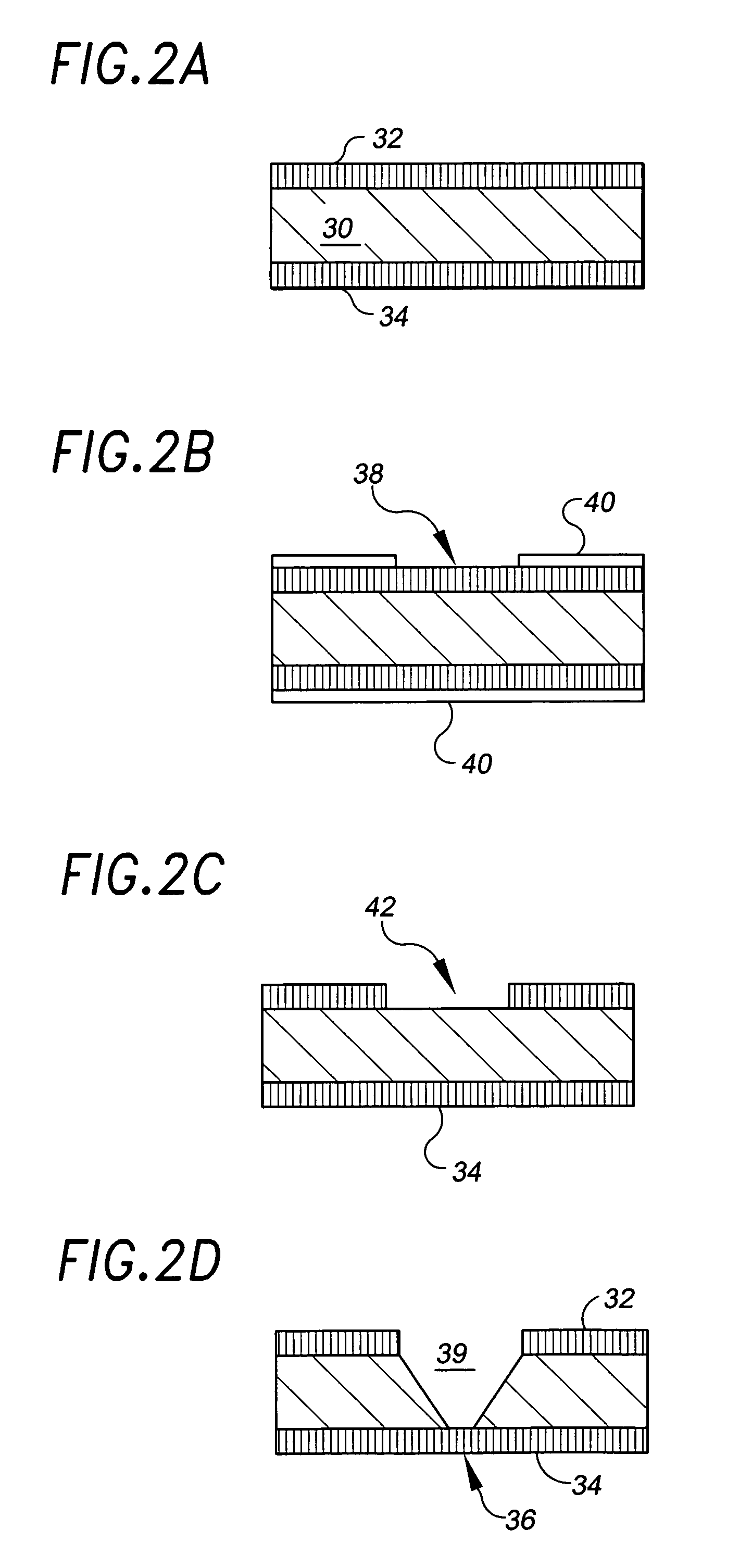
[0087]A 50 nm-thick silicon nitride membrane having a cavity formed on one surface was produced by the process outlined in FIGS. 2A-G. The silicon nitride was deposited by low pressure chemical vapor deposition. The cavity bowl was etched in the membrane by a reactive ion etch process. FIG. 4A is an electron micrograph of the cavity formed in the membrane.
[0088]The membrane surface opposite that including the cavity was exposed to an argon ion beam etch at an energy of about 3 KeV, and a flux of about 3 Ar+sec / nm2. The ion beam diameter was about 200 μm and the membrane temperature during the etch was maintained at about −120° C. The ion beam was directed toward the membrane for 1 sec during each 5 sec interval. During the etch process, ion detection and counting was carried out.
[0089]FIG. 4B is an electron micrograph of the membrane cavity including a 10 nm limiting aperture formed by thinning of the membrane. FIG. 4C is a plot of argon ion count / second as a function of sputtering ...
example 2
[0100]A silicon nitride membrane of about 50 nm in thickness was produced in the manner of FIGS. 2A-2E. An aperture was formed through the entire thickness of the membrane by reactive ion etch. This resulted in a 37 nm-wide aperture, an electron micrograph of which is shown in FIG. 5A. The membrane and aperture were then exposed to an argon ion beam at a flux of about 1.7 Ar+ / nm2 / sec and an energy of about 3 KeV. The ion beam was directed toward and away from the membrane to sputter for 1 second during each 5 second interval. The membrane was maintained at a temperature of about −102° C. during the ion beam exposure.
[0101]FIG. 5B is an electron micrograph of the 58 nm-wide aperture that resulted from 180 seconds of sputtering. FIG. 5C is a plot of counted ions / sec as a function of time. A generally linear relationship between ion counts as a function of time is demonstrated.
[0102]The invention does not require that the process being controlled by feedback be a subtractive process as...
example 3
[0121]A silicon nitride membrane of about 500 nm in thickness was produced in the manner of the process outlined in FIGS. 2A-E. An aperture was formed through the entire thickness of the membrane by reactive ion etching. FIG. 7A is an electron micrograph of the 95 nm-wide aperture that resulted from the etch.
[0122]The membrane and its aperture were then exposed to an argon ion beam flux at an energy of about 3 KeV, and a flux of about 47 Ar+ / sec / nm2. The membrane was maintained at a temperature of about 20° C. during ion flux exposure. The ion beam was directed to the membrane for 250 ms for each 1 sec time interval.
[0123]FIG. 7B is an electron micrograph of the membrane after exposure to the argon ion beam reduced the aperture diameter to about 3 nm. FIG. 7C is a plot of counted argon ions / sec as a function of time. A generally linear count rate is indicated for midpoints in the process.
[0124]Without being bound by theory, the inventors herein understand that the mechanisms underly...
PUM
| Property | Measurement | Unit |
|---|---|---|
| Electric charge | aaaaa | aaaaa |
| Current | aaaaa | aaaaa |
| Electrical conductor | aaaaa | aaaaa |
Abstract
Description
Claims
Application Information


