Feedback amplifier circuit operable at low voltage by utilizing switched operational amplifier and chopper modulator

a low-voltage, switched-operational technology, applied in the direction of dc-amplifiers with dc-coupled stages, differential amplifiers, dc-amplifiers with semiconductor devices/discharge tubes, etc., can solve the problem of increasing the dc offset voltage of the amplifier, increasing the low frequency (1/f) noise, and difficult to apply the two techniques to the low-noise amplifier by utilizing an analog switch. problem, to achieve the effect o

Inactive Publication Date: 2009-09-15
SEMICON TECH ACADEMIC RES CENT
View PDF12 Cites 24 Cited by
  • Summary
  • Abstract
  • Description
  • Claims
  • Application Information

AI Technical Summary

Benefits of technology

[0030]An essential object of the present invention is to provide a feedback amplifier circuit including a switched operational amplifier, which allows an operating point for the operational amplifier to be easily set, and which is further capable of properly canceling and compensating the offset voltage by auto-zero operation.
[0037]As described above, the feedback amplifier circuit according to the present invention includes the second capacitor which grounds the feedback point of the feedback circuit to block the DC voltage during an auto-zero operation interval and moreover accumulates and holds the offset voltage of the output terminal of the amplifier during the auto-zero operation interval, and thereafter cancels out the offset voltage of the input terminal of the amplifier by the accumulated and held offset voltage together with the first capacitor during an amplification interval subsequent to the auto-zero operation interval. Accordingly, the DC current can be blocked by the second capacitor, the operating points of the amplifier can be freely set, and further, the DC offset voltage at the input terminal of the amplifier can be canceled out during the auto-zero operation interval. Since any decrease in the DC offset voltage due to a leakage current can be compensated only by the second capacitor, the feedback amplifier circuit can be designed independent of the first capacitor of the feedback circuit. Further, since the voltage at the virtual grounding point (above-described feedback point) of the feedback circuit is grounded by the second switching device during the auto-zero interval, there occur neither on-resistances nor mismatch of clock feed-through. Thus, the influences of the DC offset voltage of the amplifier can be eliminated.

Problems solved by technology

However, in the scaled CMOS technique, increase in a direct-current (DC) offset voltage and increase in a low frequency (1 / f) noise lead to a serious problem.
The auto-zero operation technique thus makes it possible to reduce the low-frequency noises of the amplifier circuit, however, one problem of the auto-zero operation technique is to increase in a baseband noise floor caused by aliasing of a broadband noise unique to a sampling process.
The above-mentioned two techniques are required for a low noise amplifier operating at a low voltage, however, it is difficult to apply the two techniques to the low noise amplifier by utilizing an ordinary analog switch.
The reason for the difficulty is that the analog switch cannot transmit an intermediate voltage level by using a low power source voltage.
Under these conditions, there was such a problem that it was difficult to realize an electronic circuit utilizing the analog switch such as an A / D converter, a D / A converter or a DC amplifier circuit.
However, in the former case, such a device is required that has a withstand voltage higher than that of an ordinary device, and this causes problems such as complication of process, deterioration in reliability, and an increase in circuit area.
In addition, in the latter case, there are problems of an increase in a leakage current and deterioration in reliability.
In a low voltage operation for chopper stabilization, an input voltage level is unstable, and therefore, the chopper modulator 61 and the chopper demodulator 62 according to the prior art cannot be implemented in floating analog switches.
However, in the chopper amplifier circuit according to the prior art disclosed in Non-Patent Document 8, since the DC offset voltage of the operational amplifier is held in the capacitors C1, C2, it would be necessary to increase the capacitance value in order to reduce decrease in the hold voltage due to leakage, which would lead to a problem of an increase in the layout area.
Also, since the DC offset voltage is present between a pair of virtual grounding points of the fully-differential operational amplifier, there has been a problem of occurrence of an on-resistance of the chopper modulation circuit and clock feed-through mismatch (i.e., when the gate switch is turned on or off, the voltage applied to the gate causes noise to occur on the output side).

Method used


Image

  • Feedback amplifier circuit operable at low voltage by utilizing switched operational amplifier and chopper modulator
  • Feedback amplifier circuit operable at low voltage by utilizing switched operational amplifier and chopper modulator
  • Feedback amplifier circuit operable at low voltage by utilizing switched operational amplifier and chopper modulator

Examples


first preferred embodiment

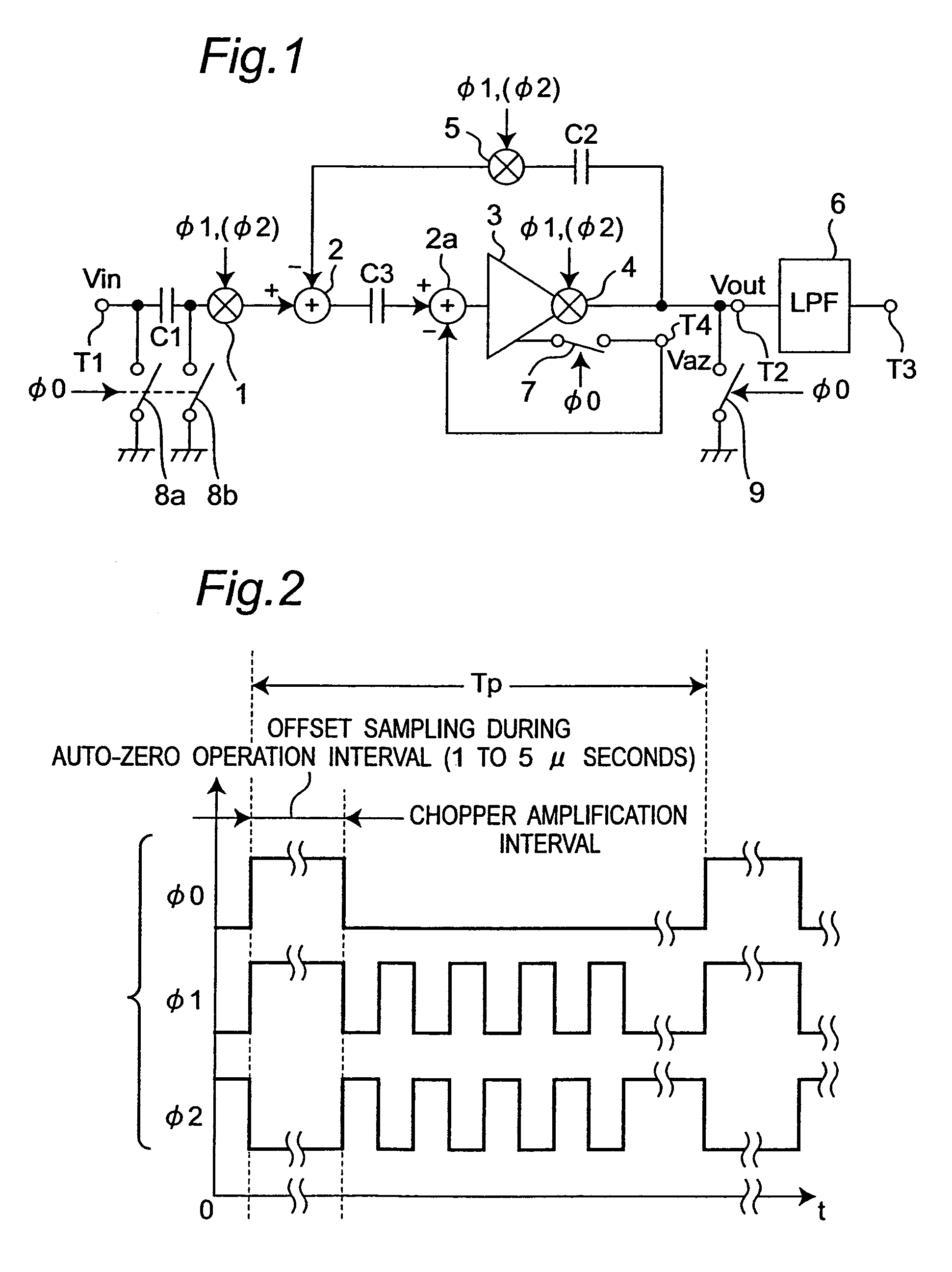
[0064]FIG. 1 is a block diagram showing a configuration of a chopper amplifier circuit according to the first preferred embodiment of the present invention. FIG. 2 is a timing chart showing control signals φ0, φ1, and φ2 for use in the chopper amplifier circuit of FIG. 1. The chopper amplifier circuit according to the first preferred embodiment, as compared with the chopper amplifier circuit according to the prior art of FIG. 22, is characterized in that the chopper amplifier circuit includes:

[0065](a) a capacitor C3 for blocking a DC current and compensating any decrease in the DC offset voltage due to a leakage current, and an adder 2a for feeding back an auto-zero operation signal Vaz, both provided between the adder 2 and the input terminal of the switched operational amplifier 3; and

[0066](b) switches 8a, 8b and 9 for grounding both ends and an output signal terminal or output terminal T2 of a capacitor C1 during an auto-zero operation interval in which the control signal φ0 ho...

second preferred embodiment

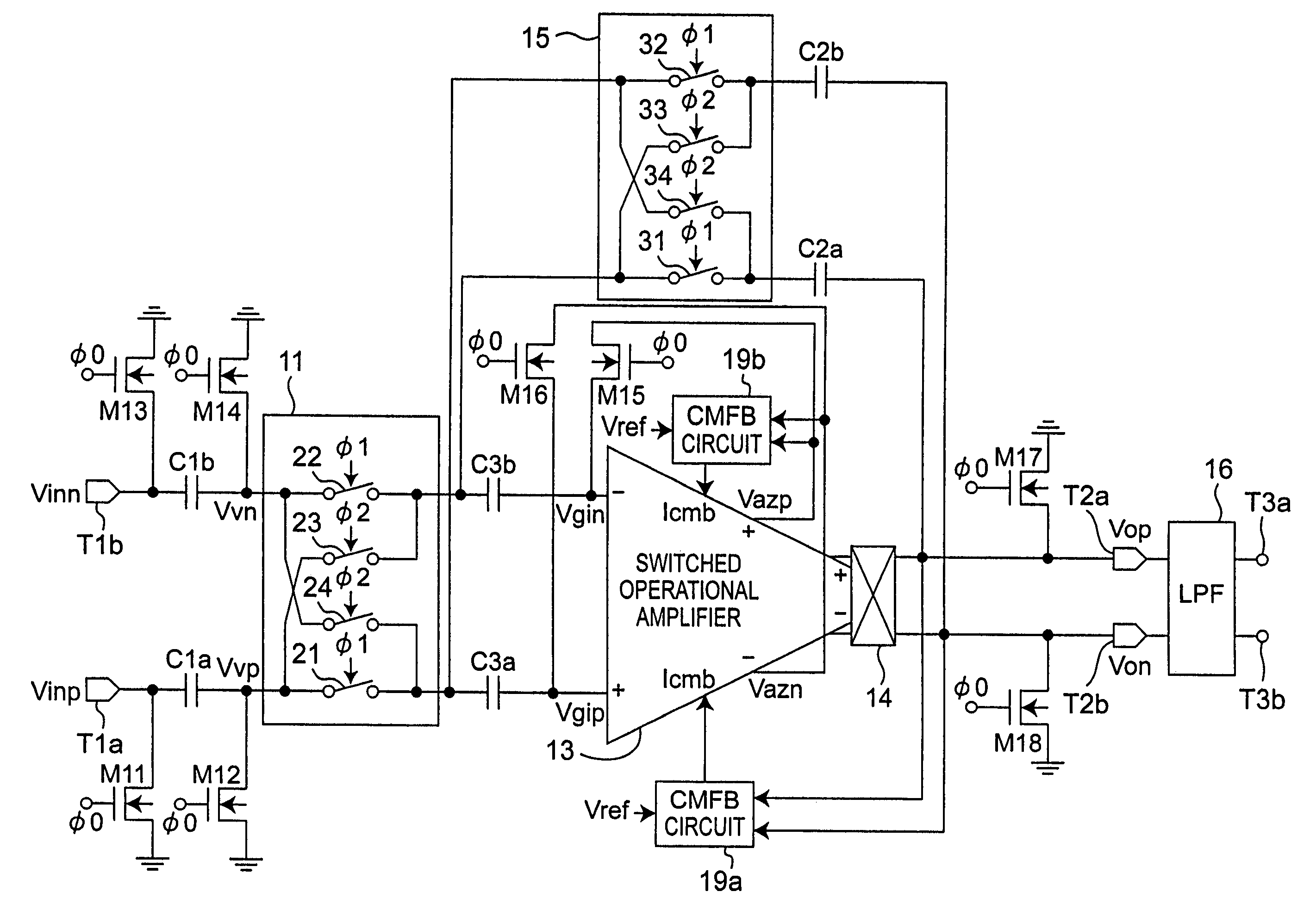
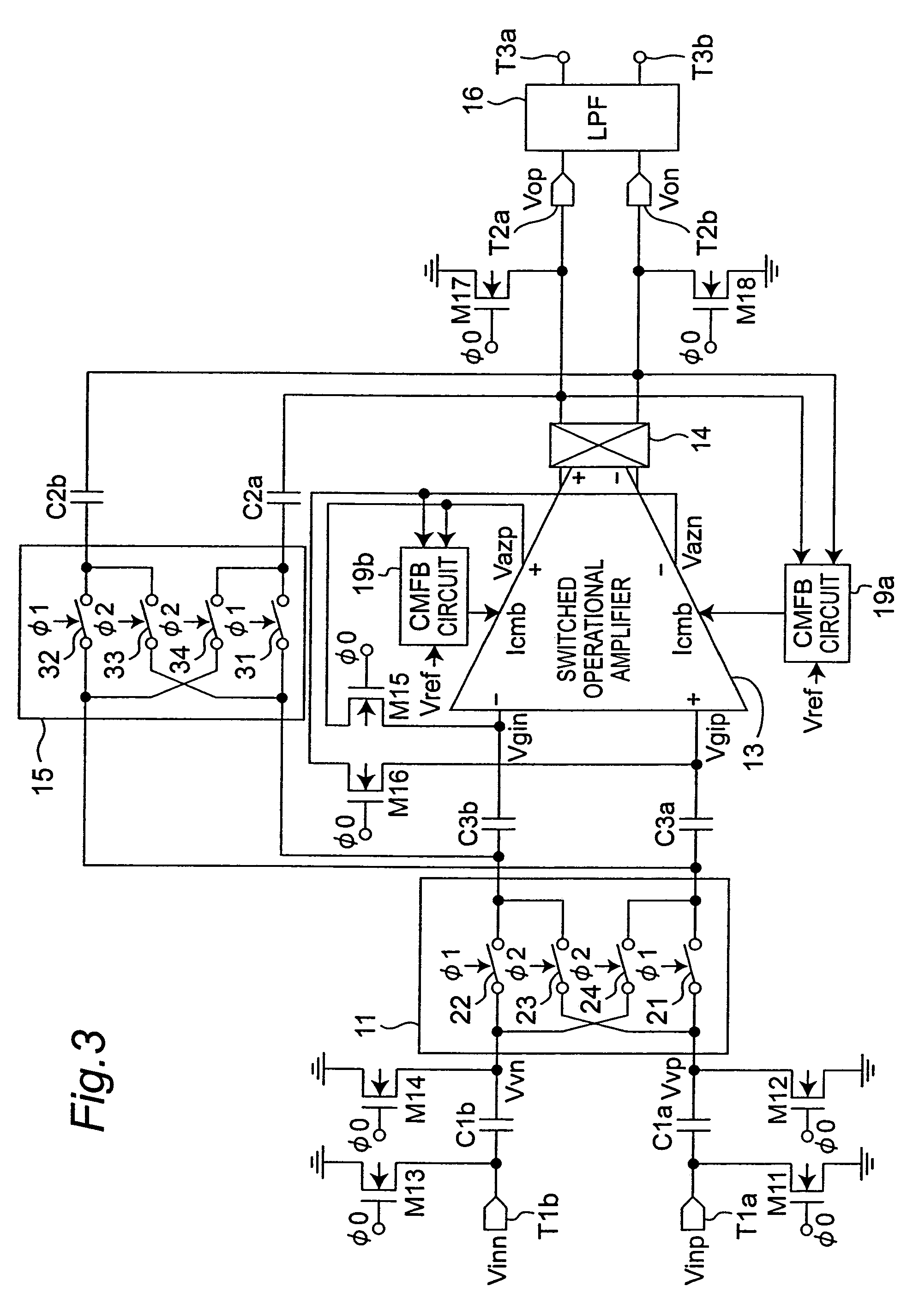
[0072]FIG. 3 is a block diagram showing a configuration of a fully-differential chopper amplifier circuit according to the second preferred embodiment of the present invention. Referring to FIG. 3, the chopper amplifier circuit according to the second preferred embodiment is characterized by realizing a chopper amplifier circuit according to the first preferred embodiment of FIG. 1 using a fully-differential amplifier. The present chopper amplifier circuit is constituted by including a chopper modulator 11, a fully differential two-input four-output switched operational amplifier 13 provided with a chopper demodulator 14 at a final stage thereof, a chopper modulator 15 for a negative feedback circuit, a low-pass filter 16, a common mode feedback circuit (referred to as a CMFB circuit hereinafter) 19, input terminals T1a and T1b, intermediate output terminals T2a and T2b, output terminals T3a and T3b, coupling capacitors C1a and C1b, capacitors C2a and C2b for the negative feedback c...

third preferred embodiment

[0088]FIG. 5 is a block diagram showing a configuration of a feedback amplifier circuit according to a third preferred embodiment of the present invention. FIG. 6 is a timing chart showing a control signal φ0 for use in the feedback amplifier circuit of FIG. 5. The feedback amplifier circuit of FIG. 5, given as an example in which the chopper amplifier circuit of FIG. 3 is applied to a common feedback amplifier circuit, is characterized in that the chopper modulators 11 and 15 and the chopper demodulator 14 are deleted in FIG. 3. In this feedback amplifier circuit, as shown in FIG. 6, signal amplification is performed after each offset sampling interval that is repeated at a predetermined cycle. According to this feedback amplifier circuit, auto-zero capacitors C3 are inserted at virtual grounding points (Vvp, Vvn) of the fully-differential switched operational amplifier 13, so that operating points (Vgip, Vgin) of the switched operational amplifier 13 can be freely set, and moreove...


PUM


Abstract

In a feedback amplifier circuit, a first switching device executes an auto-zero operation by inputting a signal outputted from an amplifier to an input terminal of the amplifier during an auto-zero operation interval prior to an amplification interval. A first capacitor accumulates and holds an offset voltage at the output terminal of the amplifier during the auto-zero operation interval, and cancels an offset voltage at the input terminal of the amplifier by an accumulated and held offset voltage during an amplification interval subsequent to the auto-zero operation interval. A second switching device grounds the feedback point of the feedback circuit during the auto-zero operation interval. A second capacitor blocks a DC voltage, and accumulates and holds an offset voltage at an output terminal of the amplifier, and cancels an offset voltage at an input terminal of the amplifier by the accumulated and held offset voltage during an amplification interval.

Description

BACKGROUND OF THE INVENTION[0001]1. Field of the Invention[0002]The present invention relates to a feedback amplifier circuit, and in particular, to a feedback amplifier circuit which is formed by, for example, a CMOS circuit, is constituted by utilizing a switched operational amplifier and a chopper modulator, and is operable at a low voltage.[0003]2. Description of the Related Art[0004]Recently, a sensor chip employing a mixed signal CMOS technique has been applied to detection and monitoring of a biological function (See, e.g., Non-Patent Documents 1 and 2). A low noise amplifier is one of the most important circuits in the sensor chip, since the sensor chip detects a low-level signal. However, in the scaled CMOS technique, increase in a direct-current (DC) offset voltage and increase in a low frequency (1 / f) noise lead to a serious problem.[0005]The auto-zero operation and chopper stabilization are techniques widely used to reduce these noises (See, e.g., Non-Patent Document 3)....

Claims


Application Information

Patent Timeline
Patent Type & Authority Patents(United States)
IPC IPC(8): H03F1/02
CPCH03F3/387H03F3/45475H03F3/45977H03F2203/45212H03F2200/261H03F2203/45136
Inventor YOSHIDA, TAKESHIMASUI, YOSHIHIROIWATA, ATSUSHIGOTOH, KUNIHIKO
Owner SEMICON TECH ACADEMIC RES CENT
Why Eureka
Try Eureka