Successive approximation analog to digital converter

a technology approximation method, which is applied in the direction of power consumption reduction, pulse technique, instruments, etc., can solve the problems of inaccuracy in the conversion, formation of transistors who conduct when their input voltage is increased, and insufficient dissipation within the device, so as to achieve the effect of increasing the output of analog to digital converter

Active Publication Date: 2009-09-15
ANALOG DEVICES INC
View PDF7 Cites 8 Cited by
  • Summary
  • Abstract
  • Description
  • Claims
  • Application Information

AI Technical Summary

Benefits of technology

[0026]This has the advantage of allowing the overlap generator to be dispensed with and consequently the switching delay introduced by the overlap generator in the prior art following a decision by the comparator is no longer incurred. This in turn means that the throughput of the analog to digital converter can be increased.
[0027]Advantageously each of the transistor switches, whether they be high side or low side switches are driven by a latch which can be latched so as to turn the transistor on or turn the transistor off. Advantageously the circuit responsible for switching a transistor into a conducting state is provided in contact with a control terminal, generally a gate, of the transistor switch such that the transistor can be switched on rapidly by that control circuit. The control circuit also has the ability to force the latch to transition to a state for holding the transistor in a conducting state. Thus, following the decision to switch a transistor on, the control signal does not incur propagation delays associated with propagating through a latch or a non-overlap generator, but instead is applied to the gate of the relevant transistor switch whilst also directly forcing the latch to transition, or alternatively causing other combinational logic to instigate a transition of the latch, to a new state. Thus not only is the switch off time for the transistors brought into the period whilst the comparator is regenerating, that is making its decision, but additionally the propagation delay between the output of the comparator and the relevant transistor switch is much reduced because the control signal does not have to propagate through a latch or through a non-overlap generator.
[0028]According to a second aspect of the present invention there is provided a successive approximation converter comprising a plurality of capacitors, wherein the switches associated with a capacitor representing a bit weight in a bit trial can be individually controlled such that a capacitor can be connected to either a first reference voltage or to a second reference voltage by electronically controlled switches, and during a bit trial the switches can be controlled such that a capacitor that is being trialled, or that will be altered for the next bit trial, is disconnected from the reference voltages prior to the completion of the bit trial so as to reduce a switching time to change a connection status of the capacitor.

Problems solved by technology

In use, it is generally considered to be undesirable for the first and second switches, that is the high side and low side switches, to be simultaneously conducting as this provides a short circuit between the first and second reference voltages which either results in unnecessary dissipation within the device and perturbs the reference voltages thereby leading to inaccuracies in the converted result.
Of course this need not be the case and use of other technologies, such as CMOS, may result in the formation of the transistors who conduct when their input voltage is low.

Method used


Image

  • Successive approximation analog to digital converter
  • Successive approximation analog to digital converter
  • Successive approximation analog to digital converter

Examples


Embodiment Construction

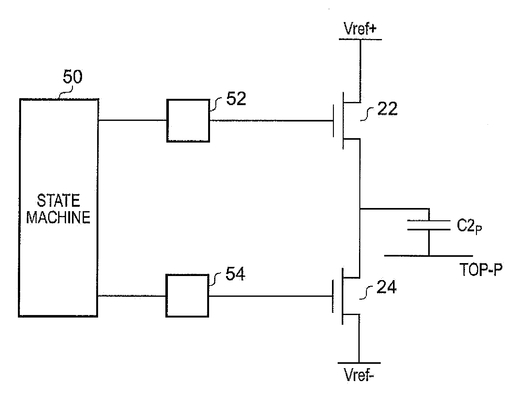
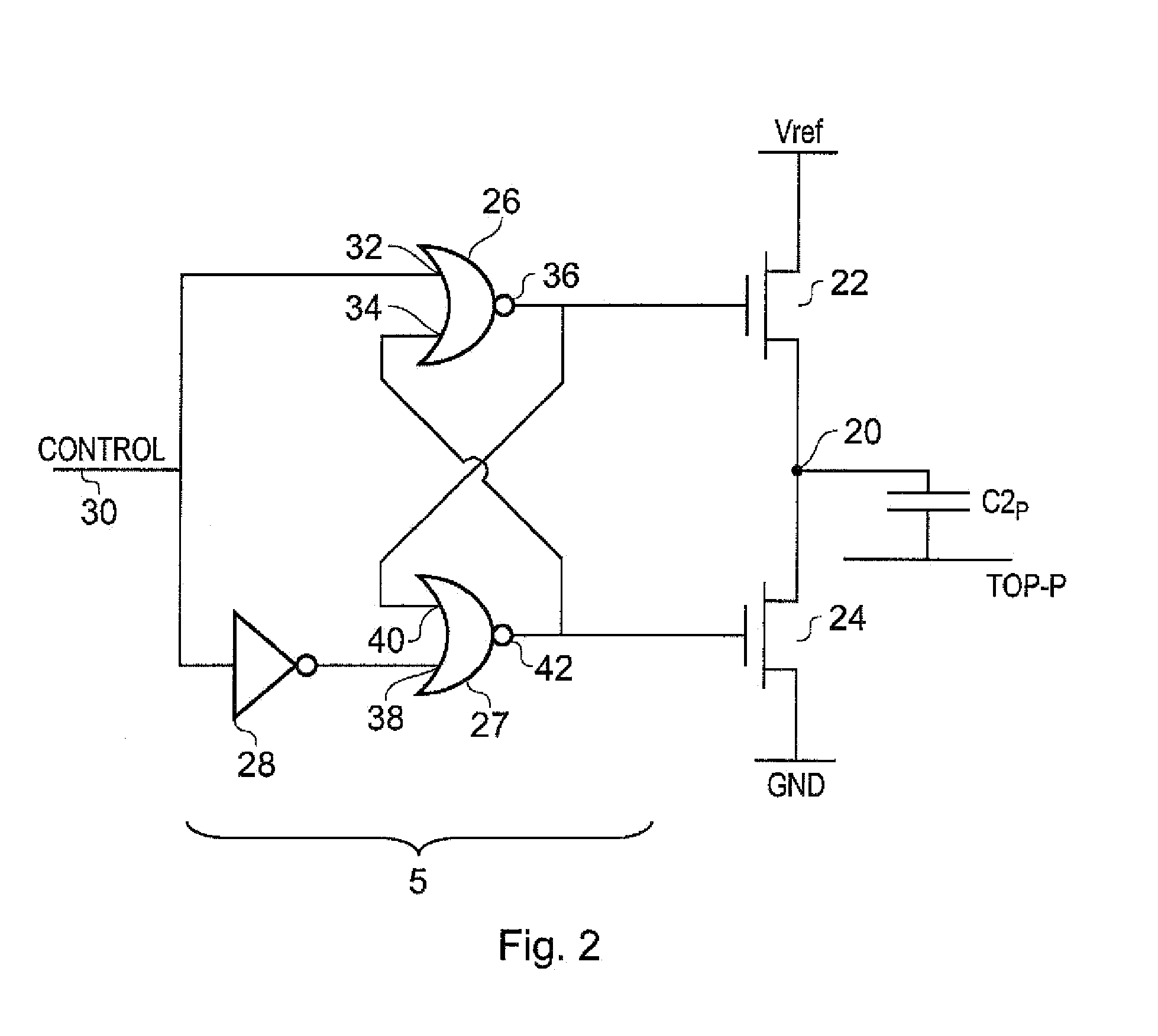
[0041]FIG. 3 schematically illustrates a drive arrangement for one pair of high side and low side switches which are used to connect a capacitor of a capacitor array to either first or second reference voltages, Vref+ and Vref− within a successive approximation converter. For simplicity, the same capacitor and switching transistors are considered in FIG. 3 as were illustrated in FIG. 2.

[0042]The sequence of transistor switching performed as part of the successive approximation conversion process is controlled by a state machine 50 which selects which capacitors are to be trialled, and hence which transistors are to be selected for potential switching within any given bit trial. Each transistor has an associated transistor control circuit of which circuit 52 is arranged to control transistor 22 and the circuit 54 is arranged to control transistor 24. The circuits 52 and 54 may receive their control signals solely from the state machine 50 or, as shown in FIG. 4, they may incorporate ...


PUM


Abstract

A successive approximation analog to digital converter comprising a plurality of capacitors which during a successive approximation conversion are selectively connectable to a first reference or a second reference under the command of a controller. During a conversion step where the connections of a given capacitor may be varied, the switches to the given capacitor are both placed in a high impedance state during a decision period of a comparator.

Description

[0001]This application claims priority under 35 U.S.C. § 119(e) to U.S. Provisional Application Ser. No. 60 / 830,414, entitle “SUCCESSIVE APPROXIMATION ANALOG TO DIGITAL CONVERTER,” filed on Jul. 12, 2006, which is herein incorporated by reference in its entirety.FIELD OF THE INVENTION[0002]The present invention relates to a successive approximation Analog to Digital Converter, and in particular to a converter where the sequence for controlling switches connecting capacitors in a capacitor array to first or second reference voltages has been modified so as to improve the speed of the analog to digital converter.BACKGROUND OF THE INVENTION[0003]Successive approximation converters using switched capacitor arrays are well known.[0004]An example of an idealized differential input successive approximation switched capacitor analog to digital converter is shown in FIG. 1. This converter receives a differential signal on its signal inputs Vinp and Vinn, and fixed inputs Vref, and GND. The V...

Claims


Application Information

Patent Timeline
Patent Type & Authority Patents(United States)
IPC IPC(8): H03M1/34
CPCH03K17/04123H03K17/162H03K17/6872H03K19/0013H03M1/0863H03M1/462H03M1/466H03M1/468H03M1/002H03M1/804
Inventor HURRELL, CHRISTOPHER PETER
Owner ANALOG DEVICES INC
Why Eureka
Try Eureka