Wire grid polarizer and liquid crystal display device using the polarizer

a technology of liquid crystal display device and wire grid, which is applied in the direction of optics, instruments, optical elements, etc., can solve the problems of insufficient degree of polarization in a short-wavelength region of visible light, 120 nm or less, and the difficulty of microstructural concave-convex grid implementation, etc., to achieve the effect of easy removal

Active Publication Date: 2009-10-20
ASAHI KASEI KK
View PDF15 Cites 112 Cited by
  • Summary
  • Abstract
  • Description
  • Claims
  • Application Information

AI Technical Summary

Benefits of technology

[0056]Preparation of a COP plate with a concavo-convex grid shape transferred thereto.
[0057]Prepared was a nickel stamper having on the surface a concavo-convex grid with the height of the concavo-convex grid of 230 nm. The concavo-convex grid was made by patterning using the laser interference exposure method, sinusoidal shape in cross section and streak grid shape in upper face. The dimensions of the plane were 500 mm both in length and width. Using the nickel stamper, the concavo-convex grid shape was transferred to the surface of a cycloolefin resin (hereinafter, abbreviated as COP) plate with a thickness of 0.5 mm and length and width of 520 mm by hot press method, and a COP plate with the concavo-convex grid shape transferred thereto was thus prepared. The glass transition temperature (Tg) of the COP was 105° C.
[0058]More specifically, hot press was performed as described below. First, a pressing machine was evacuated, and the nickel stamper and COP plate were heated to 190° C. After the nickel stamper and COP plate reached 190° C., the concavo-convex grid of the nickel stamper was transferred to the COP plate at a pressing pressure of 2 Mpa for four minutes of pressing time. Further, with the pressing pressure kept at 2 MPa, the nickel stamper and COP plate were cooled to 40° C., the vacuum was released, and then, the pressing pressure was released. When the pressing pressure was released, the nickel stamper and COP plate were easily removed. The surface shape of the COP plate with the concavo-convex grid shape transferred thereto was observed using a field-emission scanning electron microscope (hereinafter, abbreviated as FE-SEM) and it was confirmed that the concavo-convex grid shape of the nickel stamper was transferred faithfully.
[0060]Next, the COP plate with the concavo-convex grid shape transferred thereto was cut into 520 mm×460 mm rectangles to be COP plates for drawing as drawing target members. At this point, the plates were cut so that the longitudinal direction (520 mm) of the 520 mm×460 mm rectangle was substantially parallel with the longitudinal direction of the concavo-convex grid.
[0061]Silicon oil was coated on surfaces of the COP plates for drawing by spray, and placed in a circular air oven at about 80° C. for 30 minutes. Next, the COP plate for drawing was fixed by chucks of a drawing machine at its opposite ends of 10 mm in the longitudinal direction, and placed in this stat in a circular air oven with the temperature adjusted to 113±1° C. for 10 minutes. Then, drawing was performed at speed of 250 mm / min, and finished when the distance between the chucks was drawn by five times, and twenty seconds later, the drawn COP plate was placed in an atmosphere of room temperature, and cooled with the distance between the chucks kept. The drawn COP plate was almost uniformly constricted at about 40% of the center portion, and the width of the most shrank portion was 200 mm. Similarly, the COP plates were drawn while changing only the distance between the chucks to 3.5 times and 2.5 times, and the minimum widths of the center portions of the drawn COP plates were 240 mm and 280 mm, respectively.
[0062]The surface and cross section of each of these three types of drawn COP plates were observed by FE-SEM, and it was understood that the pitch and height of the microstructural concavo-convex grid of each of the plates were 100 nm / 95 nm (pitch / height), 120 nm / 113 nm, or 140 nm / 133 nm, the cross section was in the sinusoidal shape, the shape from the upper face was a streak-shaped grid shape, and that the plates were shrank substantially in similar figures to the concavo-convex grid shape prior to the drawing.

Problems solved by technology

However, in the existing photolithography technique, it has been difficult to implement a microstructural concavo-convex grid with pitches of the level of 120 nm or less in a large area of 100 cm2 or more.
However, the above-mentioned wire grid polarizer needs to consider resonance in the visible light spectrum when the polarizer is used as a diffraction grating, and has a problem that a sufficient degree of polarization is not obtained in a short-wavelength region of the visible light.

Method used


Image

  • Wire grid polarizer and liquid crystal display device using the polarizer
  • Wire grid polarizer and liquid crystal display device using the polarizer
  • Wire grid polarizer and liquid crystal display device using the polarizer

Examples


Embodiment Construction

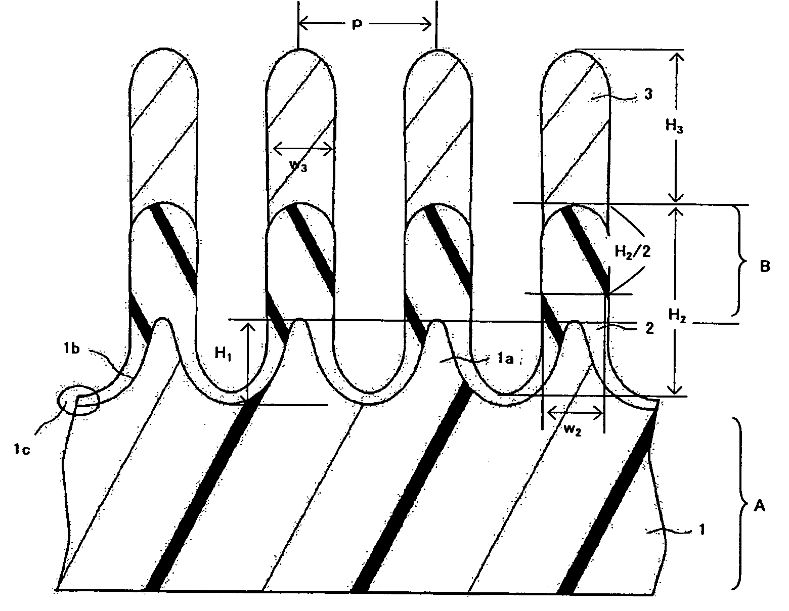
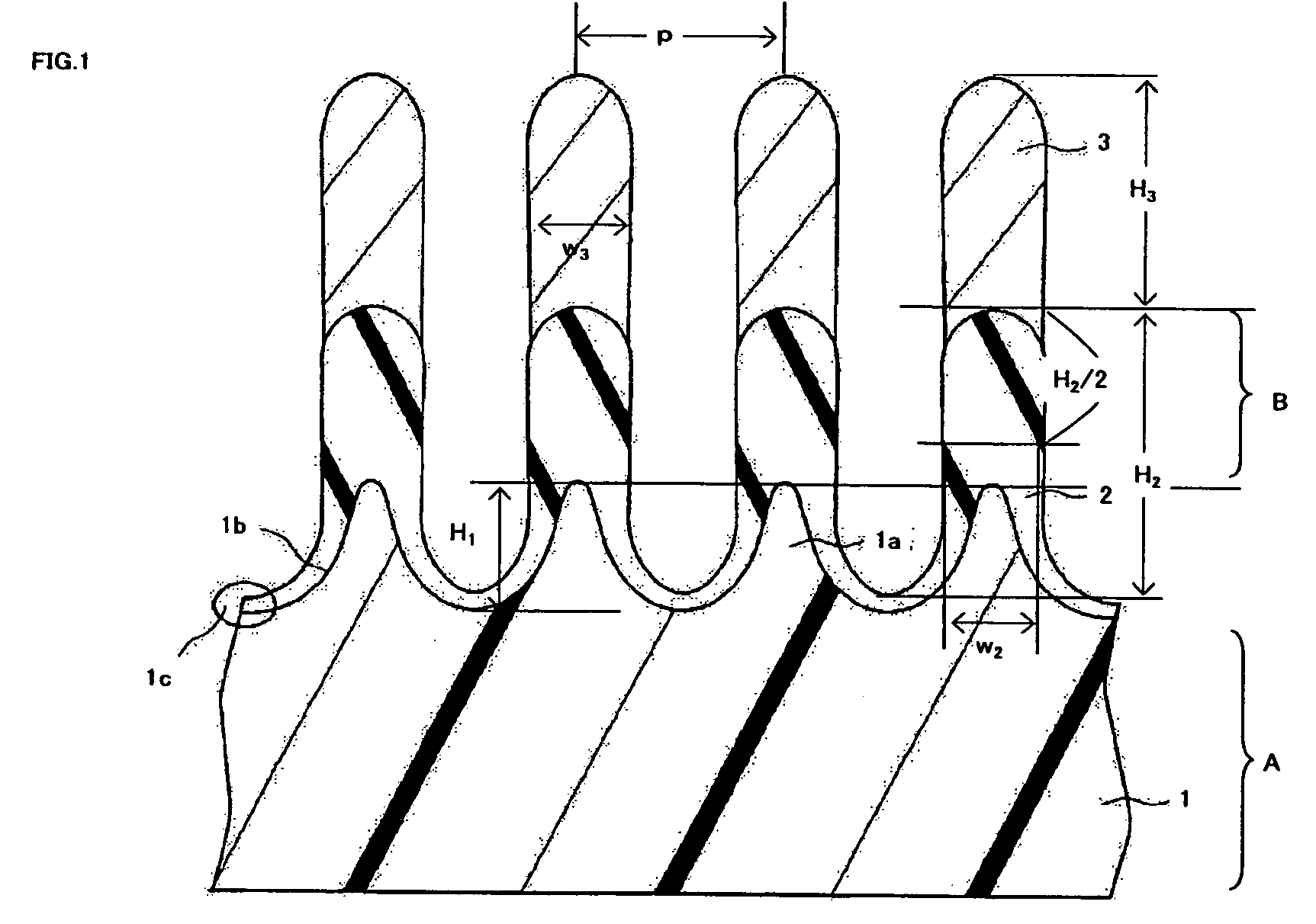
[0029]FIG. 1 is a schematic cross-sectional view showing part of a wire grid polarizer according to an embodiment of the invention. The wire grid polarizer as shown in FIG. 1 is mainly comprised of a resin substrate 1 having grid-shaped convex portions, a dielectric layer 2 provided to cover the grid-shaped convex portions 1a (hereinafter, simply referred to as convex portions 1a as appropriate) of the resin substrate and part of side faces 1b of the convex portions 1a, and metal wires 3 provided on the dielectric layer.

[0030]A resin for use in the resin substrate 1 is required to be a resin substantially transparent in the visible region. Examples of such a resin include amorphous thermoplastic resins such as a poly methyl methacrylate resin, poly carbonate resin, polystyrene resin, cycloolefin resin (COP), cross-linked polyethylene resin, polyvinyl chloride resin, polyallylate resin, polyphenylene ether resin, modified polyphenylene ether, polyether imide resin, polyether sulfone ...


PUM

PropertyMeasurementUnit
wavelengthsaaaaaaaaaa
areaaaaaaaaaaa
wavelengthsaaaaaaaaaa

Abstract

A wire grid polarizer has a resin substrate having grid-shaped convex portions, a dielectric layer provided to cover the grid-shaped convex portions of the resin substrate and at least part of side faces of the portions, and metal wires provided on the dielectric layer. The wire grid polarizer has a microstructural concavo-convex grid structure having grid-shaped convex portions, is not limited in structure, and has both the excellent degree of polarization and excellent transmittance over a wide range in the visible region.

Description

BACKGROUND OF THE INVENTION[0001]1. Field of the Invention[0002]The present invention relates to a wire grid polarizer and liquid crystal display device using the wire grid polarizer.[0003]2. Related Background Art[0004]The recent development of photolithography technique has enabled formation of a microstructural pattern with pitches of the level of the wavelength of light. Members and products with such extremely small pitches are of wide application and useful not only in the semiconductor field but also in the optical field.[0005]For example, in a wire grid where conductor lines comprised of metal and the like are arranged in the shape of a grid with specific pitches on a substrate, when the pitches are remarkably smaller than (for example, less than half) the incident light (for example, visible light with wavelengths of 400 nm to 800 nm), the wire grid reflects almost all the electric field vector component of the light vibrating in parallel with the conductor lines, while all...

Claims


Application Information

Patent Timeline
Patent Type & Authority Patents(United States)
IPC IPC(8): G02F1/1335
CPCG02B5/3058G02F1/133536G02F2001/133548G02F1/133548
Inventor YAMAKI, HIROSHISATO, YUSUKENAMATAME, TAKUJIKAWAZU, YASUYUKI
Owner ASAHI KASEI KK
Why Eureka
Try Eureka