Method of fabrication of normally-off field-effect semiconductor device

a semiconductor device and field-effect technology, applied in the field of field-effect semiconductor devices, can solve the problems of reducing the electron concentration in the two-dimensional electron gas layer, inconvenient use of conventional normally-on hemt, and unnecessary associated circuitry, and achieves the effect of reducing the turn-on resistance of the normally-off device, fine adjustment, and easy operation

Inactive Publication Date: 2009-11-10
SANKEN ELECTRIC CO LTD
View PDF15 Cites 8 Cited by
  • Summary
  • Abstract
  • Description
  • Claims
  • Application Information

AI Technical Summary

Benefits of technology

[0018]The notched or otherwise indented surfaces of the two semiconductor layers are created purely epitaxially, rather than by etching, a possible alternative, which unavoidably involves degradation of crystallinity. Grown epitaxially, with lateral overgrowth utilized for creation of slant-surfaced sections, the semiconductor layers are notable for fewer dislocations and excellent crystallinity. Thus the present invention succeeds in making the field-effect semiconductor device normally off without in any way sacrificing its performance.
[0020]The threshold of the device varies with the angle of a slanting surface or surfaces of the slant-surfaced sections of the semiconductor layers. That angle, then, is controllable in terms of the growth rates of the semiconductor layers. The threshold of the device is capable of easy, fine adjustment.
[0021]Either part or all of the slant-surfaced section of the second semiconductor layer may be made thinner than the rest of that layer, so much so that the device is infallibly made normally off. The other, thicker parts of the second semiconductor layer serve to make the associated two-dimensional carrier gas layer higher in carrier concentration and so to lower the turn-on resistance of the normally-off device.

Problems solved by technology

Use of such a negative power supply made the associated circuitry unnecessary complex and expensive.
The conventional normally-on HEMT was rather inconvenient of use.
A thinner electron supply layer weakens the electric field due to piezoelectric depolarization caused by the heterojunction between electron supply layer and electron transit layer, resulting in the diminution of electron concentration in the two-dimensional electron gas layer.
The normally-off HEMT based upon this conventional scheme proved to possess its own drawback, however.
The result was an inconveniently high drain-source turn-on resistance.
The selective etching of the electron supply layer is objectionable because it is likely to lead to the impairment of the semiconductor crystal structures of both electron supply layer and electron transit layer.
Selectively etching the electron supply layer without causing these inconveniences was indeed highly difficult, and the resulting HEMTs were not necessarily satisfactory in performance.
This proposed construction is not necessarily reliable for stable HEMT operation in normally-off mode.

Method used


Image

  • Method of fabrication of normally-off field-effect semiconductor device
  • Method of fabrication of normally-off field-effect semiconductor device
  • Method of fabrication of normally-off field-effect semiconductor device

Examples


embodiment

of FIG. 7

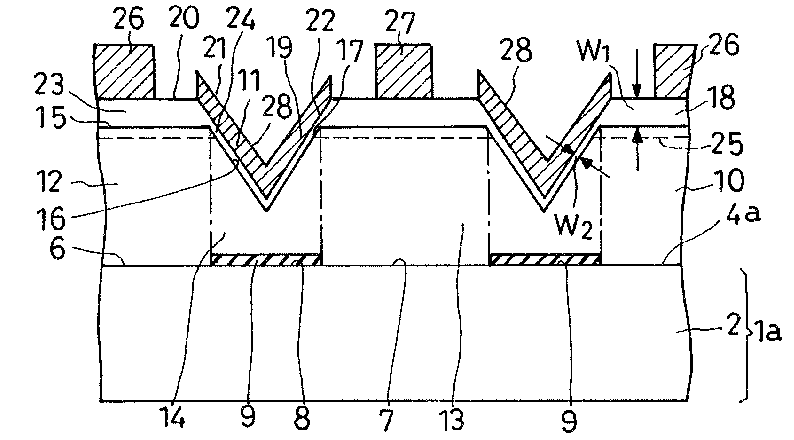
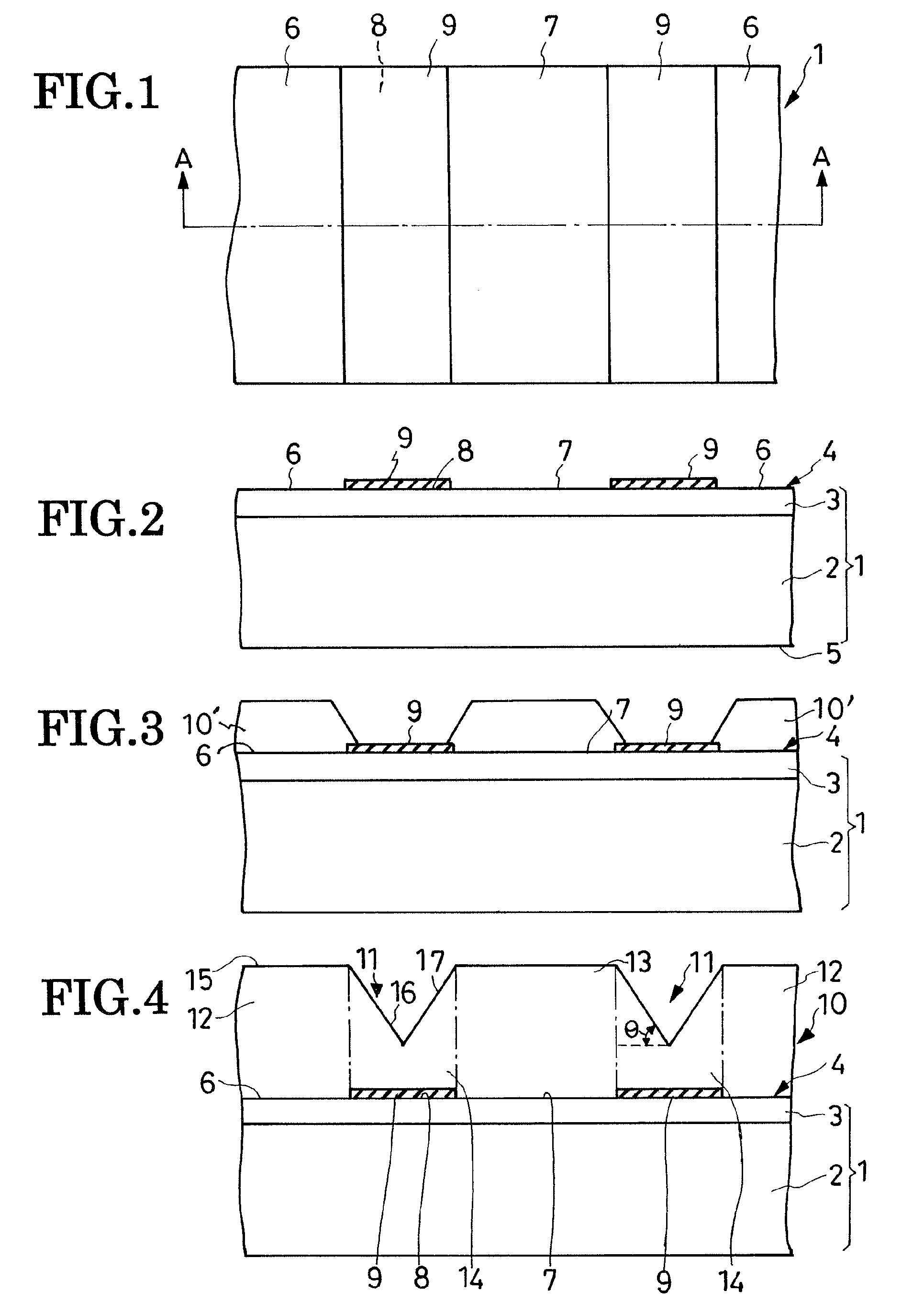
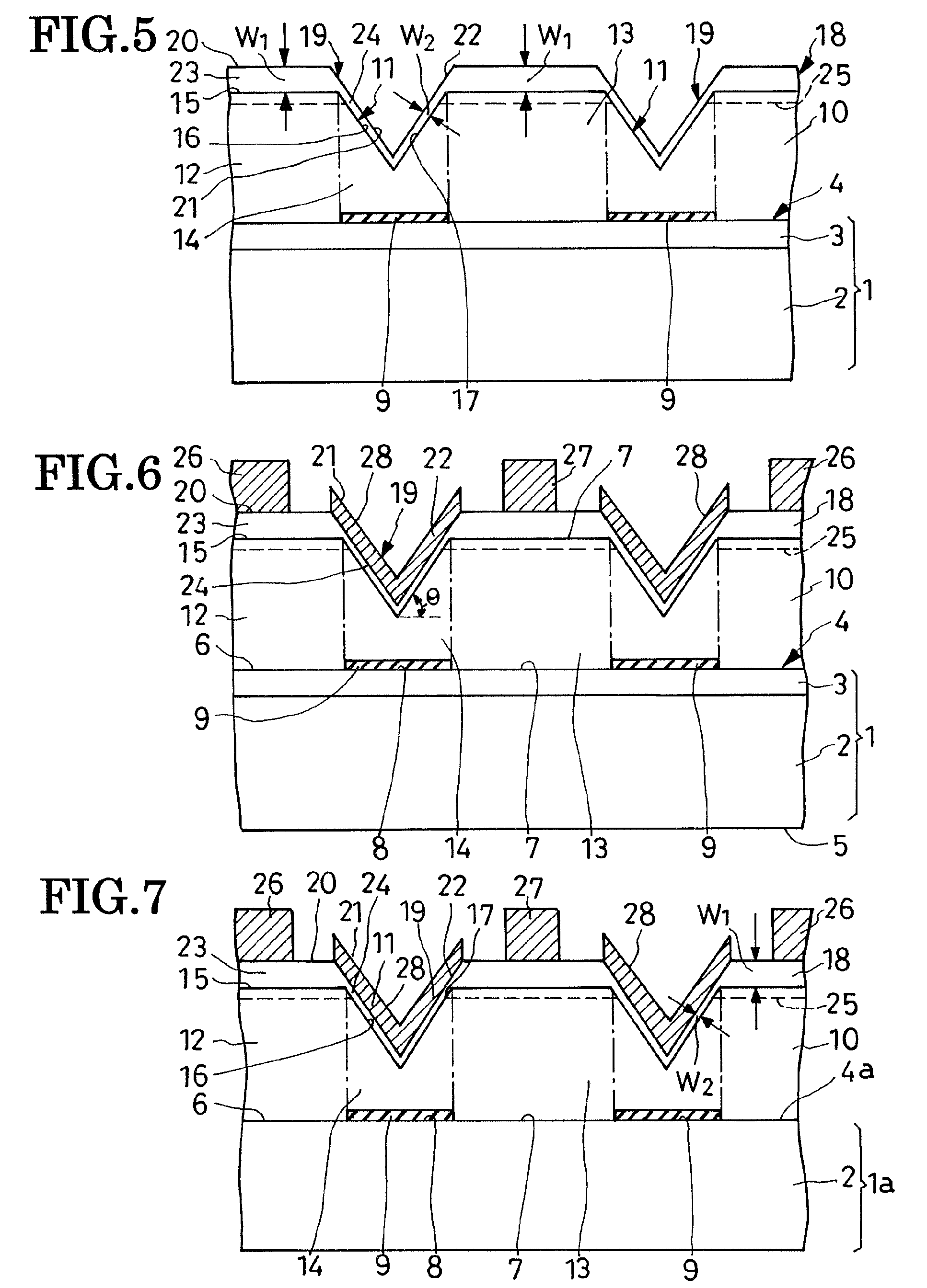
[0077]The HEMT shown here differs from that of FIG. 6 only in the absence of the buffer 3, FIG. 2, from its substrate 1a. This substrate 1a is therefore a single layer 2 of silicon throughout.

[0078]The antigrowth masks 9 directly overlie the silicon substrate 1a. These masks 9 and the other constituents of the HEMT, identified by the same reference characters as their counterparts in FIG. 6, are made by the same methods as set forth above with reference to FIGS. 1-6. This embodiment offers the advantage, in addition to all those enumerated above, that all the semiconductor growth processes needed for the HEMT fabrication can be streamlined. An independent buffer might be interposed between substrate 1a and electron transit layer 10, though.

Embodiment of FIGS. 8-10

[0079]The third preferred form of HEMTs are shown in two different stages of fabrication in FIGS. 8 and 9 and completed in FIG. 10. This embodiment features a quasi-V-notch 11a, FIGS. 9 and 10, in an electron trans...


PUM


Abstract

A normally-off HEMT is made by first providing a substrate having its surface partly covered with an antigrowth mask. Gallium nitride is grown by epitaxy on the masked surface of the substrate to provide an electron transit layer comprised of two flat-surfaced sections and a V-notch-surfaced section therebetween. The flat-surfaced sections are formed on unmasked parts of the substrate surface whereas the V-notch-surfaced section, defining a V-sectioned notch, is created by lateral overgrowth onto the antigrowth mask. Aluminum gallium nitride is then deposited on the electron transit layer to provide an electron supply layer which is likewise comprised of two flat-surfaced sections and a V-notch-surfaced section therebetween. The flat-surfaced sections of the electron supply layer are sufficiently thick to normally generate two-dimensional electron gas layers due to heterojunctions thereof with the first and the second flat-surfaced section of the electron transit layer. The V-notch-surfaced section of the electron supply layer is not so thick, normally creating an interruption in the two-dimensional electron gas layer.

Description

CROSS REFERENCE TO RELATED APPLICATIONS[0001]This application claims priority to Japanese Patent Application No. 2007-178390, filed Jul. 6, 2007.BACKGROUND OF THE INVENTION[0002]This invention relates to semiconductor devices, particularly to field-effect semiconductor devices as typified by the high electron mobility transistor (HEMT), and more particularly to such field-effect semiconductor devices that operate normally off. The invention also pertains to a method of fabricating such normally-off field-effect semiconductor devices.[0003]HEMTs have been known which are made from semiconducting nitrides belonging to Groups III-V compounds. Japanese Unexamined Patent Publication No. 2005-158889 is hereby cited as dealing with this type of semiconductor devices which are pertinent to this invention. The prior art HEMT comprises an electron transit layer of undoped gallium nitride (GaN) grown on a silicon substrate via a buffer layer, and an electron supply layer of n-type aluminum gal...

Claims


Application Information

Patent Timeline
Patent Type & Authority Patents(United States)
IPC IPC(8): H01L21/336
CPCH01L29/42316H01L29/7789H01L29/7787H01L29/66462H01L29/2003H01L29/0657
Inventor SATO, KEN
Owner SANKEN ELECTRIC CO LTD
Why Eureka
Try Eureka