Wafer-level packaging cutting method capable of protecting contact pads

a cutting method and packaging technology, applied in semiconductor devices, forming microstructural systems, semiconductor/solid-state device details, etc., can solve the problems of not being suitable for batch production, and the packaging process is rather tedious, so as to reduce the damage and contamination, reduce the yield damage, and simplify the dicing process

Inactive Publication Date: 2009-11-24
TESSERA ADVANCED TECH
View PDF4 Cites 0 Cited by
  • Summary
  • Abstract
  • Description
  • Claims
  • Application Information

AI Technical Summary

Benefits of technology

[0006]A main object of the present invention is to provide a cutting method for wafer-level packaging capable of protecting the contact pads for improving product yield and reliability.
[0008]This cutting method for wafer-level packaging is able to simplify the dicing process, reduce the damages and contamination due to the cutting process, and is suitable for packaging of typical electronic devices, MEMS devices, and optical devices that effectively reduces the yield damages resulted from the subsequent procedures (such as wafer dicing, breaking, washing . . . etc). Furthermore, this technology is applicable for typical semiconductor manufacturing processes, suitable for batch production, possesses ease for inspection, has higher yield rate superiority, and is able to overcome difficulties encountered by conventional technology.

Problems solved by technology

The disadvantages of the above are the following: the size of the packaging die as produced by this packaging method is bigger than desired, the packaging process is rather tedious, and does not lend itself to befitting the current electronic product appeals of having thinner and smaller devices, and also requiring individualized operations, such as even manual operations, and is not suitable for batch production.
Furthermore, the bottleneck for this packaging technology often occurred during the later dicing process, in which outside mechanical forces can lead to structural damages, and the micro-particles generated during the cutting process can lead to product contamination, thereby reducing yield.

Method used


Image

  • Wafer-level packaging cutting method capable of protecting contact pads
  • Wafer-level packaging cutting method capable of protecting contact pads
  • Wafer-level packaging cutting method capable of protecting contact pads

Examples


Embodiment Construction

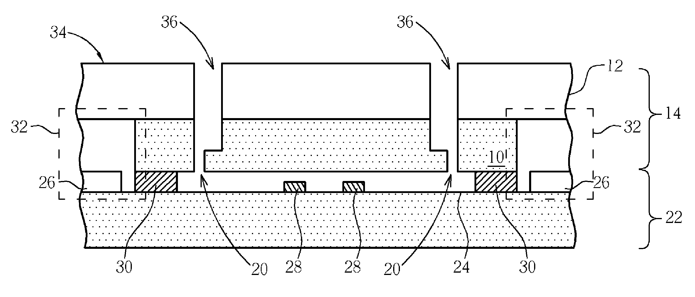
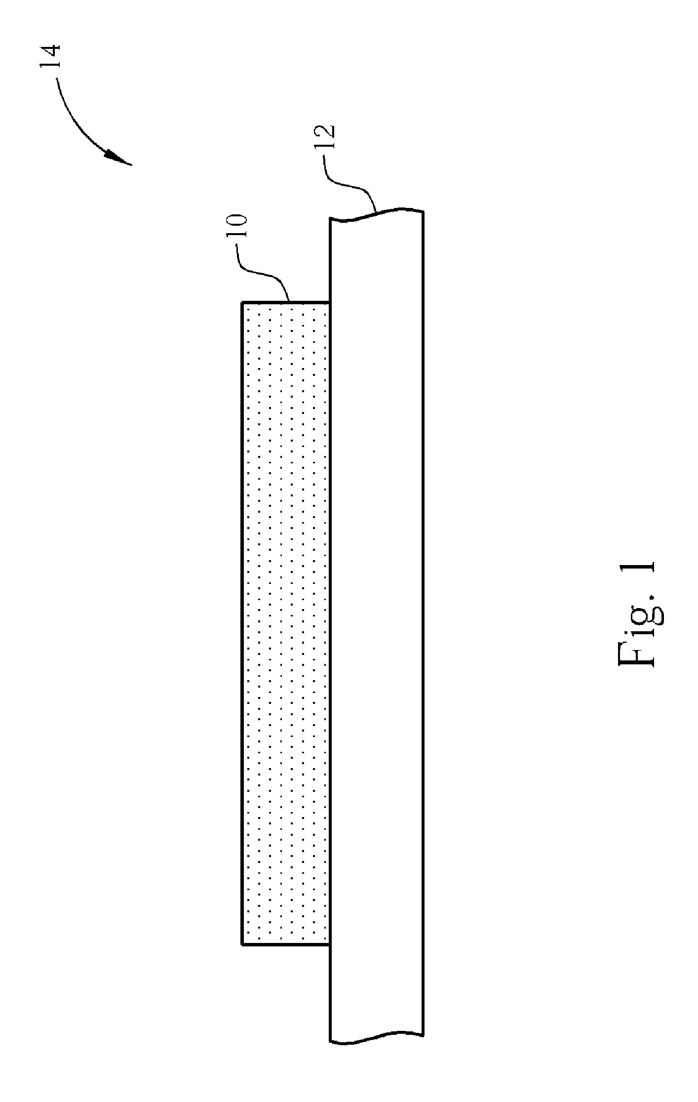
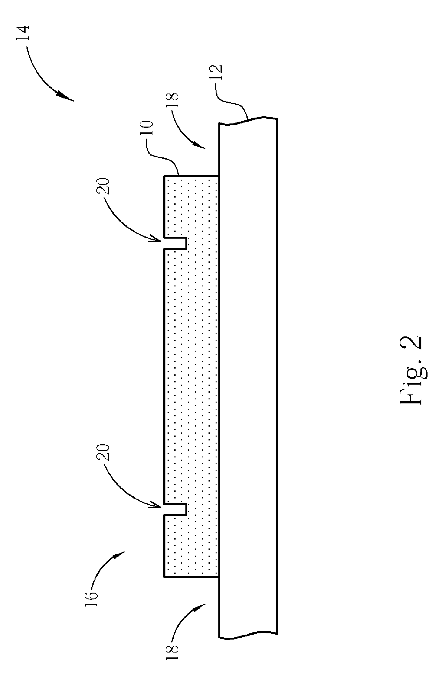
[0012]Referring from FIG. 1 to FIG. 6, FIGS. 1-6 are the illustrative schematics showing a wafer dicing method in accordance with a preferred embodiment of the present invention. As shown in FIG. 1, a first wafer 10 and a second wafer 12 are provided. Through anodic bonding, eutectic bonding, fusion bonding, plasma activation bonding, and other conventional wafer bonding processes, the first wafer 10 and the second wafer 12 are bonded to form a cap wafer 14. The first wafer 10 can be a standard wafer, a silicon wafer, or a patterned wafer; the second wafer 12 can be a glass wafer or a packaging wafer, a silicon wafer, or wafers of other materials. Furthermore, the choice for the cap wafer 14 is not limited to only the selection of the two-piece bonded wafer as illustrated in the present preferred embodiment, but whereas, a single-piece standard wafer or silicon wafer can also be used as the cap wafer 14.

[0013]As shown in FIG. 2, a surface patterning process is performed. On a front ...


PUM


Abstract

A cutting method for wafer-level packaging capable of protecting the contact pad, in which several cavities and precutting lines are formed at the front surface of a cap wafer, and the depth of each precutting line is lesser than the thickness of the cap wafer, followed by the bonding of the cap wafer to the device wafer, which has several devices and several bonding pads disposed on the surface of the device wafer, followed by performing a wafer dicing process, along the precutting lines cutting through the cap wafer, and after removing a portion of the cap wafer that is not bonded to the device wafer, for exposing the bonding pads at the surface of the device wafer, and finally performing a dicing process for forming many packaged dies.

Description

BACKGROUND OF THE INVENTION[0001]1. Field of the Invention[0002]The present invention is related to a cutting method for wafer-level packaging capable for protecting the contact pads, in particularly, to a cutting method for wafer-level packaging able to simplify the dicing process, improve the yield, and protect the contact pad when forming a precutting line on the cap wafer.[0003]2. Description of the Prior Art[0004]The semiconductor device packaging process is an important procedure, the so-called packaging is in reference to the sealing and encapsulating of the core structure inside the device, the function of the packaging is to protect the fragile semiconductor devices (such as for example, optical devices, MEMS devices, etc) against the outside environmental attacks (such as mechanical damage or micro-particle contamination, etc), and to provide the structural support and signal transmission functions.[0005]The conventional packaging procedure is as follows. First, the proces...

Claims


Application Information

Patent Timeline
Patent Type & Authority Patents(United States)
IPC IPC(8): H01L21/44
CPCB81C1/00873H01L23/10B81C2203/0118H01L23/3114H01L2924/0002H01L2924/00
Inventor TSAI, CHUN-WEISHAO, SHIH-FENG
Owner TESSERA ADVANCED TECH
Why Eureka
Try Eureka