Device isolation technology on semiconductor substrate

Active Publication Date: 2009-11-24
ASM JAPAN
View PDF39 Cites 398 Cited by
  • Summary
  • Abstract
  • Description
  • Claims
  • Application Information

AI Technical Summary

Problems solved by technology

The above described conventional LOCOS technique has a number of disadvantages, which become rather unacceptable when attempting to apply this technique to the fabrication of sub-micron devices.
First, the oxidization of silicon happens not only in the vertical direction but also in the horizontal direction.
Secondly, due to the stresses caused by the bird's beak effect, a part of nitride hard mask in the compressed regions of silicon nitride layer diffuses to adjacent tensile strained regions at the interface of the pad oxide layer and the substrate, and forms a silicon-nitride-like region.
Wh

Method used


Image

  • Device isolation technology on semiconductor substrate
  • Device isolation technology on semiconductor substrate
  • Device isolation technology on semiconductor substrate

Examples


example 1

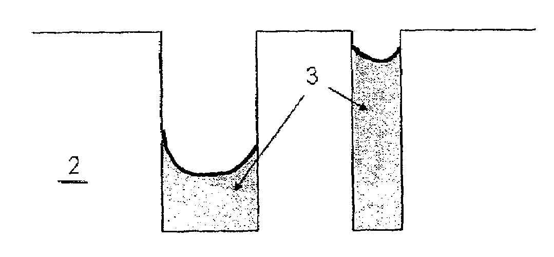
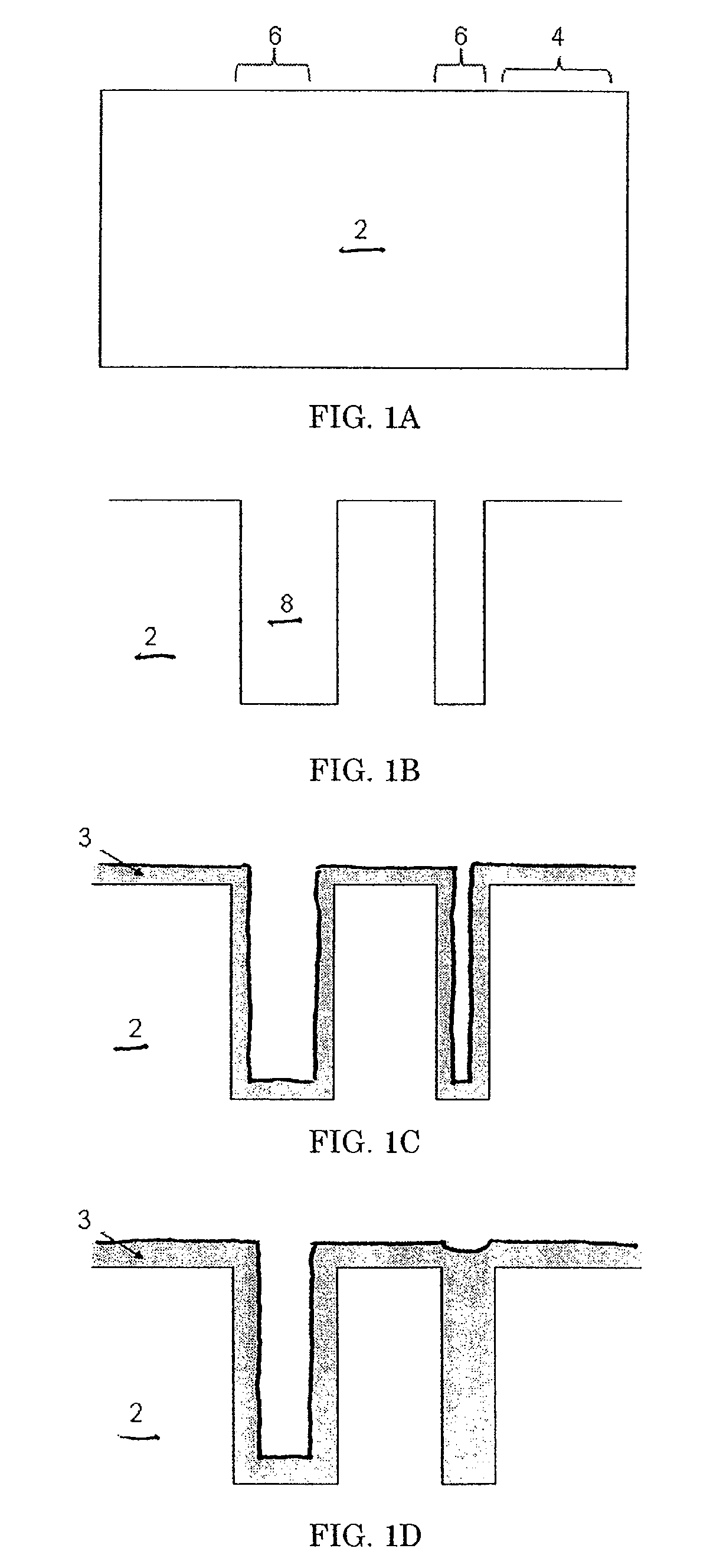
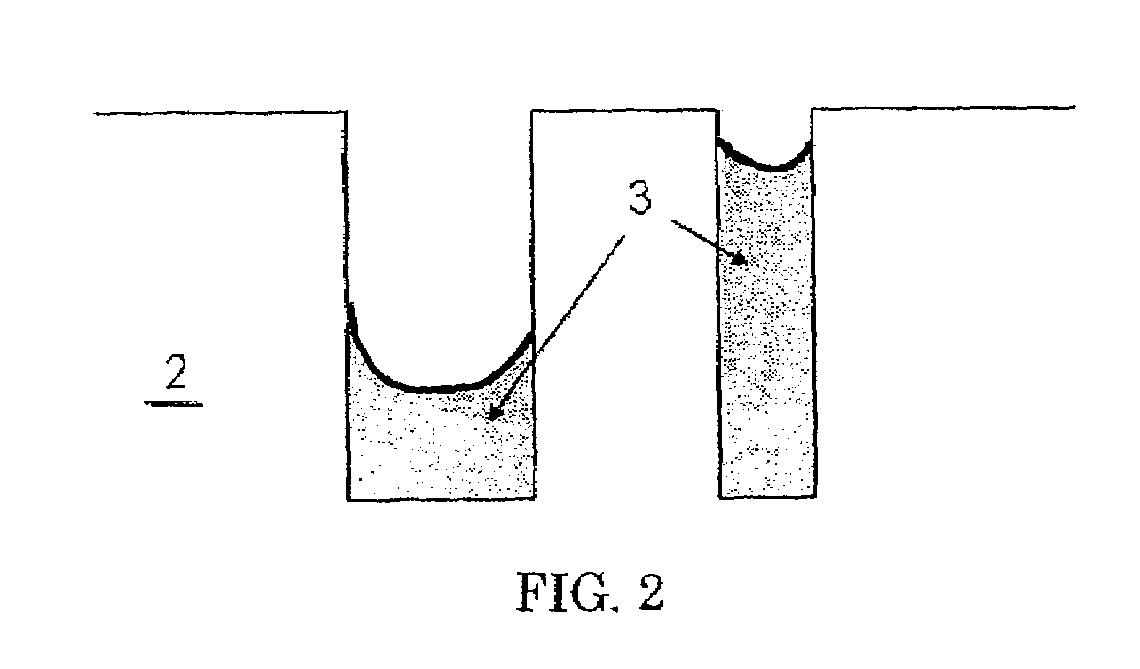
[0052]With reference to the features of FIGS. 1 and 2, an insulative layer 3 was formed by introducing SiH4, n-hexane and nitrogen gas into a reaction chamber for CVD processing wherein a semiconductor substrate 2 having trenches 8 was placed. The trenches included relatively wide trenches (a width of 500 m and a depth of 350 nm) and relatively narrow trenches (a width of 50 nm and a depth of 350 nm). The flow rates of SiH4, n-hexane, and nitrogen gas are shown in Table 1. No oxidizing gas was used. RF power (a frequency of 13.56 MHz, 200 W) was applied to generate plasma over the substrate 2. The SiH4 and solvent reacted in the presence of the inert gas on the surface of the semiconductor substrate 2 having the trenches 8 to form the insulative layer 3. The semiconductor substrate 2 may be maintained at a temperature ranging from approximately 0° C. to 200° C. by placing the semiconductor substrate 2 on a chuck maintained at that temperature. In this example, the semiconductor subs...

example 2

[0056]An insulative layer 3 was formed by introducing SiH4, TMDSZ and NH3 into a reaction chamber for CVD processing wherein a semiconductor substrate 2 having trenches 8 was placed. The trenches included relatively wide trenches (a width of 500 nm and a depth of 350 nm) and relatively narrow trenches (a width of 50 nm and a depth of 350 nm). The flow rates of SiH4, n-hexane, and nitrogen gas are shown in Table 2. No oxidizing gas was used. RF power (a frequency of 13.56 MHz, 200 W) was applied to generate plasma over the substrate 2. The SiH4 and TMDSZ reacted in the presence of the NH3 gas on the surface of the semiconductor substrate 2 having the trenches 8 to form the insulative layer 3. The semiconductor substrate 2 may be maintained at a temperature ranging from approximately 0° C. to 200° C. by placing the semiconductor substrate 2 on a chuck maintained at that temperature. In this example, the semiconductor substrate 2 may be maintained at a temperature of approximately 30° ...

example 3

[0061]To determine the chemical bonding and compositions of multi-step cured insulative layers, the insulative layers 3 were deposited on a blanket wafer by PECVD at 30° C. according to the processes described in Example 1. The multi-step curing was comprised of oxygen-containing treatment (baking), oxygen UV curing, and thermal annealing, which were conducted as follows:

[0062]Baking:

[0063]Oxygen gas: 3 slm

[0064]Nitrogen gas: 1 slm

[0065]Temperature: 400° C.

[0066]Duration: 1 minute

[0067]Pressure: 800 Pa

[0068]UV Curing:

[0069]UV lamp: Xe lamp (100 mW / cm2)

[0070]Oxygen gas: 3 slm

[0071]Nitrogen gas: 1 slm

[0072]Temperature: 430° C.

[0073]Duration: 2 minutes

[0074]Pressure: 1200 Pa

[0075]Thermal Annealing:

[0076]Oxygen gas: 3 slm

[0077]Nitrogen gas: 1 slm

[0078]Temperature: 430° C.

[0079]Duration: 30 minutes

[0080]Pressure: 800 Pa

[0081]FIGS. 3 and 4 are Fourier-transform infrared absorption spectra (FTIR) analysis of insulative layers 3 deposited as described above. FIG. 3 shows the as-deposited re...


PUM


Abstract

A method of forming device isolation regions on a trench-formed silicon substrate and removing residual carbon therefrom includes providing a flowable, insulative material constituted by silicon, carbon, nitrogen, hydrogen, oxygen or any combination of two or more thereof; forming a thin insulative layer, by using the flowable, insulative material, in a trench located on a semiconductor substrate wherein the flowable, insulative material forms a conformal coating in a silicon and nitrogen rich condition whereas in a carbon rich condition, the flowable, insulative material vertically grows from the bottom of the trenches; and removing the residual carbon deposits from the flowable, insulative material by multi-step curing, such as O2 thermal annealing, ozone UV curing followed by N2 thermal annealing.

Description

BACKGROUND OF THE INVENTION[0001]1. Field of the Invention[0002]The present invention relates to the field of semiconductor integrated circuit manufacturing and, more particularly to a method of forming device isolation regions on a semiconductor substrate by using PECVD and to a method of removing residual carbon deposits from an intermediate semiconductor device structure.[0003]2. Description of the Related Art[0004]Integrated circuits fabricated on semiconductor substrates for large scale integration require multiple levels of metal interconnections to electrically interconnect the discrete layers of semiconductor devices on the semiconductor chips. Today several million devices can be fabricated in a single chip, for example, the mega-bit memory chips which are commonly used today in personal mobile and in other applications.[0005]Devices of semiconductor typically include semiconductor substrate and a plurality of adjacent, active devices that are electrically isolated from one...

Claims


Application Information

Patent Timeline
IPC IPC(8): H01L21/76H01L21/20H01L21/205H01L21/36H01L21/469
CPCH01L21/02126H01L21/02211H01L21/02222H01L21/76229H01L21/02337H01L21/02348H01L21/31604H01L21/02274
Inventor LEE, WOO JINFUKAZAWA, ATSUKIMATSUKI, NOBUO
Owner ASM JAPAN
Why Eureka
Try Eureka