Photonic funnels and anisotropic waveguides for subdiffraction light compression and pulse management at the nanoscale

a funnel and anisotropic waveguide technology, applied in the field of optical devices, can solve the problems of limiting the efficiency of coupling between nano- and micro-domains, limiting the resolution and sensitivity of near-field microscopes, and preventing the fabrication of ultra-compact all-optical processing circuits. , to achieve the effect of improving the efficiency of energy transfer and limiting energy

Inactive Publication Date: 2009-11-24
THE STATE OF OREGON ACTING BY & THROUGH THE OREGON STATE BOARD OF HIGHER EDUCATION ON BEHALF OF OREGON STATE UNIV
View PDF17 Cites 24 Cited by
  • Summary
  • Abstract
  • Description
  • Claims
  • Application Information

AI Technical Summary

Benefits of technology

[0009]The present invention relates to a waveguide device and method that supports volume propagation modes of electromagnetic waves even when the waveguide radius is significantly smaller than the free-space wavelength. The waveguide can be tapered to provide efficient coupling to and from the nanoscale with 10% or more efficiency. For example, a photonic funnel is a waveguide with cross-sectional dimensions progressively decreasing along the direction of mode propagation, concentrating light energy to the nanoscale. The waveguides of the present invention are characterized by a nonmagnetic, nonresonant core material having a highly anisotropic dielectric constant with either positive or negative refractive index. Such a core material may be realized as a nano-layered metamaterial, e.g., alternating layers of dielectric and metallic layers. The dielectric layers can be gain regions to provide amplification or loss suppression and / or to introduce a versatile control over group velocity of optical pulses in the waveguide. Specific exemplary material systems are provided for five different operational frequencies (near IR: Si / Ag, mid IR: Si / SiC, far IR: doped InGaAs / AlInAs). The waveguide designs of the present invention may use a mode structure identical to that in conventional optical waveguides, allowing for efficient energy transfer therebetween. As an example, the metamaterial waveguide core can be realized as a 1D photonic crystal (PC) medium, e.g., periodic array of thin dielectric and metallic layers. Both positive and negative refractive index structures are proposed, as well as the combination of different refractive indices to provide phase manipulation.
[0012]In one of its aspects, the present invention provides a waveguide for the propagation of light of a given wavelength, wherein: 1) the waveguide core is a nonmagnetic, nonresonant material with an anisotropic dielectric constant formed by either homogeneous material (such as Sapphire or bismuth, for example), or by a metamaterial, for example constructed from material layers oriented perpendicular to the direction of propagation, 2) the cross-sectional dimension of the waveguide is less than the wavelength in at least one portion of the waveguide, and 3) the waveguide supports the propagation of volume modes limited to a single direction along a waveguide axis. More specifically, the present invention also provides such a multi-layer waveguide with a tapered cross-sectional dimension for coupling light to subwavelength regions and / or with gain regions to modulate group velocity of radiation at the nanoscale, i.e., a PC-core waveguide photonic funnel. The tapered waveguide may have arbitrary cross-section. A metallic waveguide cladding may be used to provide better confinement of energy. Variations and extensions to the waveguides of the present invention include modification of the pulse propagation through the system (e.g., to achieve slow or fast light), coupling to free space sources, and shape optimization to further increase the efficiency of the energy transfer.

Problems solved by technology

Compressing the light beyond the diffraction limit is one of the most fundamental problems of modern photonics and plasmonics.
Such a huge scale difference introduces fundamental limitations on (i) the size of waveguiding structures and (ii) efficiency of coupling between nano- and micro-domains.
These limitations, in turn, restrict the resolution and sensitivity of near-field microscopes, prevent fabrication of ultra-compact all-optical processing circuits, integrated optoelectronic devices and other photonic systems.
However, despite the ever-increasing number of opportunities offered by modern technology, straightforward reduction of size of conventional dielectric waveguides is not possible since the onset of diffraction will lead to either cut-off of waveguide modes or to their leakage into the dielectric surrounding.
However, both these approaches have their limitations.
Therefore, excitation of SPPs requires fabrication of special kinds of coupling structures which can introduce substantial energy loss.
Exponential decay associated with evanescent waves, on the other hand, severely deteriorates the signal-to-noise ratio, limiting the minimum power required to operate the systems and maximum separation between the transmitter and receiver in these structures.
Although some approaches involving resonant excitation of surface modes in negative-index or negative-permittivity systems have been promised to restore the evanescent waves, all practical realizations of these structures are so far limited to the near-field proximity of the sub-wavelength source.
Hence, current waveguide technology is unable to effectively confine propagating electromagnetic waves to the regions substantially smaller than half of the optical wavelength (typically, about 300 nm).
State of the art plasmonic and plasmon enhanced waveguides are capable of transferring energy to subwavelength scales, but due to the incompatibility of the mode structure with free-space radiation, typically, only 0.5% of initial energy reaches the tip of a fiber in modern near-field couplers.

Method used


Image

  • Photonic funnels and anisotropic waveguides for subdiffraction light compression and pulse management at the nanoscale
  • Photonic funnels and anisotropic waveguides for subdiffraction light compression and pulse management at the nanoscale
  • Photonic funnels and anisotropic waveguides for subdiffraction light compression and pulse management at the nanoscale

Examples


Embodiment Construction

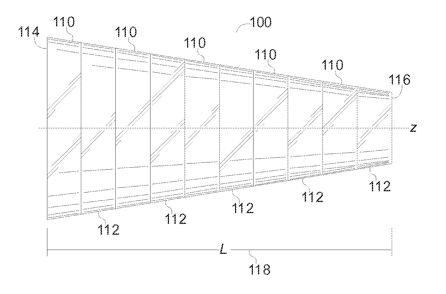
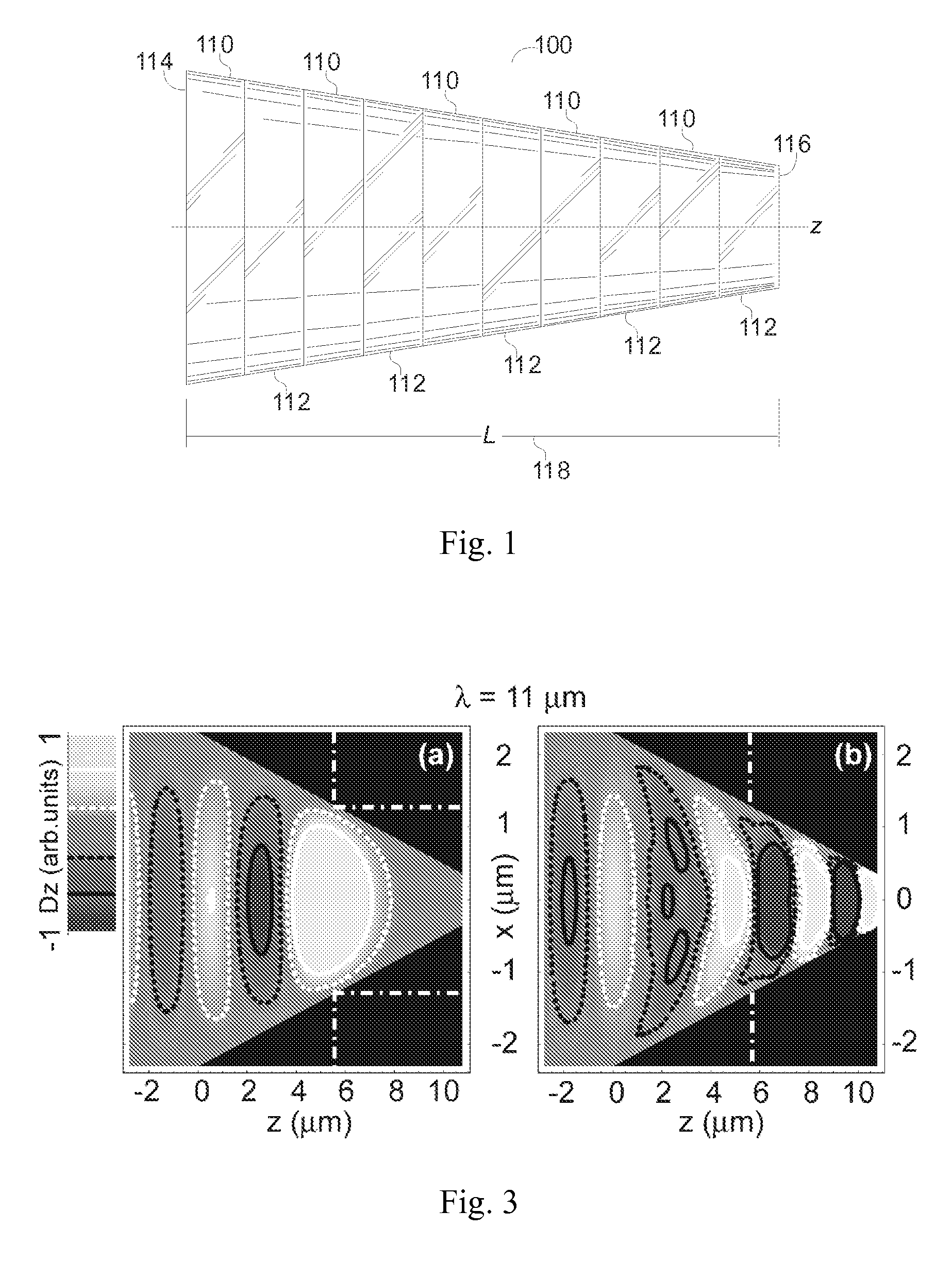
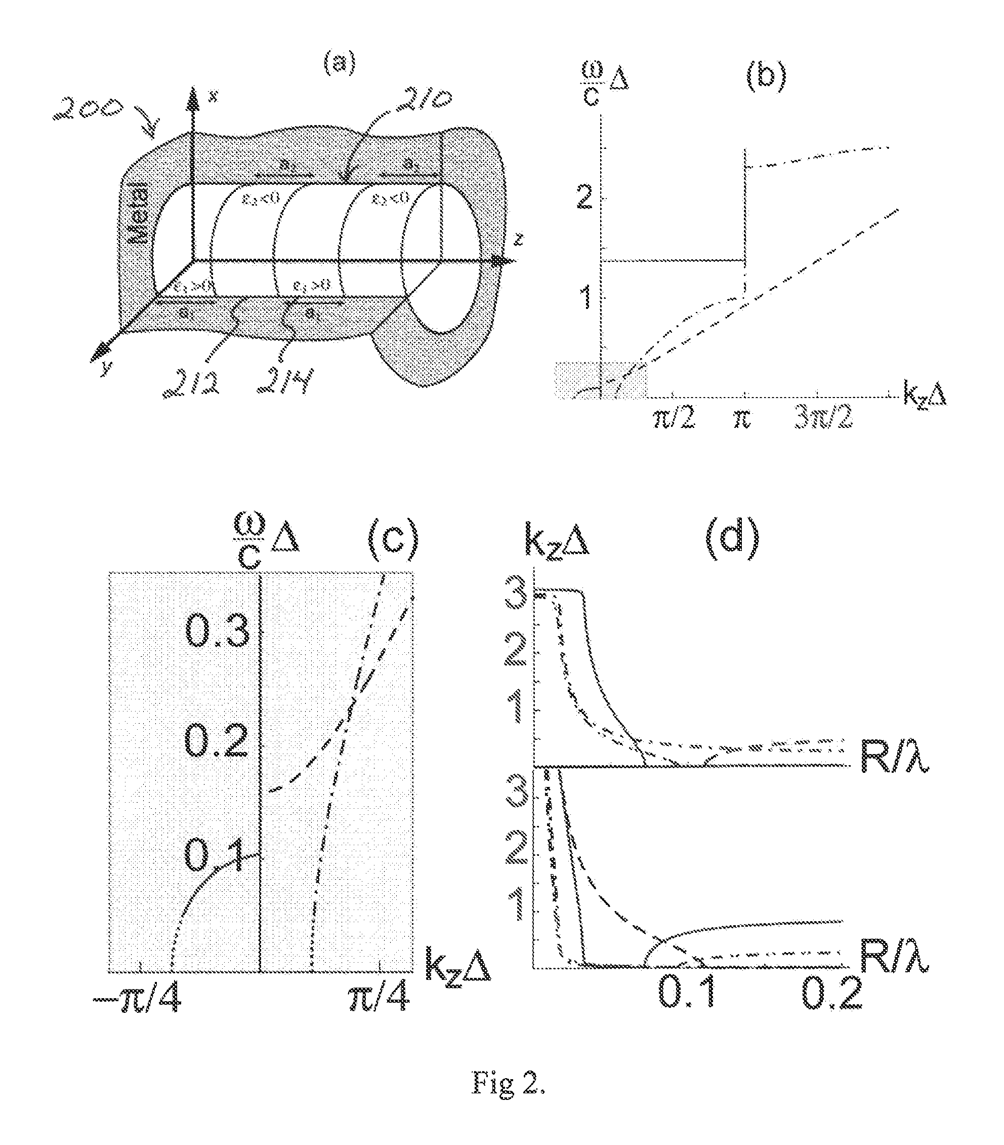
[0041]Referring now to the figures, the present invention provides a photonic funnel 100 for compressing light of a selected wavelength, λ, beyond the diffraction limit, FIG. 1. The photonic funnel 100 is able to compress light beyond the diffraction limit by inclusion of a plurality of material layers 110, 112 of differing dielectric constant oriented along the longitudinal axis of the photonic funnel with each layer having a thickness on the order of λ / 100, e.g., a metamaterial or a 1-D photonic crystal. For example, the plurality of material layers may comprise alternating layers of a dielectric (∈>0) material and a metallic (∈100 in accordance with the present invention includes a first funnel end 114 and a relatively smaller second opposing funnel end 116 to provide a tapered or optionally conical shape, with the second end having a cross-sectional dimension less than λ. In order to specify designs under which the light may be compressed to the sub-λ scale, analyses of wave pro...


PUM


Abstract

The present invention provides an apparatus for propagating electromagnetic radiation of a selected vacuum wavelength beyond the diffraction limit. The apparatus comprises a waveguide core and a cladding disposed about the core. The waveguide core may include a material with an anisotropic dielectric permittivity, with the optical axis of the material primarily aligned with direction of light propagation. In addition, the waveguide core may have a cross-sectional dimension smaller than about ½ of the selected wavelength at least at one portion of the waveguide core. The cross-sectional dimension of the waveguide core may decrease along the length of the waveguide core creating a taper to provide a photonic funnel. The waveguide core may comprise a homogeneous anisotropic material, anisotropic metamaterial, or a photonic crystal.

Description

RELATED APPLICATIONS[0001]This application claims the benefit of priority of U.S. Provisional Application No. 60 / 844,906, filed on Sep. 14, 2006, the entire contents of which application(s) are incorporated herein by reference.FIELD OF THE INVENTION[0002]The present invention relates generally to optical devices and more particularly but not exclusively to techniques and devices for manipulating electromagnetic radiation at subwavelength scales.BACKGROUND OF THE INVENTION[0003]Compressing the light beyond the diffraction limit is one of the most fundamental problems of modern photonics and plasmonics. Efficient coupling between diffraction-limited and sub-diffraction scales will strongly benefit the areas of near-field sensing, nm-scale optical control, single-molecule spectroscopy, high-energy focusing and compact optoelectronics. While light emission by atoms, molecules, quantum wells, quantum dots and other quantum objects occurs from nm-sized regions, light propagation takes pla...

Claims


Application Information

Patent Timeline
Patent Type & Authority Patents(United States)
IPC IPC(8): G02B6/26
CPCB82Y20/00G02B6/14G02B6/1228G02B6/1225
Inventor PODOLSKIY, VIKTOR A.GOVYADINOV, ALEXANDER A.
Owner THE STATE OF OREGON ACTING BY & THROUGH THE OREGON STATE BOARD OF HIGHER EDUCATION ON BEHALF OF OREGON STATE UNIV
Why Eureka
Try Eureka