Integrated trench MOSFET and junction barrier schottky rectifier with trench contact structures

a technology of junction barrier and trench contact structure, which is applied in the field of cell structure, device configuration and fabrication process of power semiconductor devices, can solve the problems of trench schottky diodes occupying additional space for planar contact, trench schottky diodes further suffering from a high leakage between drain and source, and achieve the effect of improving the configuration of semiconductor power devices

Active Publication Date: 2009-12-01
FORCE MOS TECH CO LTD
View PDF3 Cites 23 Cited by
  • Summary
  • Abstract
  • Description
  • Claims
  • Application Information

AI Technical Summary

Benefits of technology

[0009]It is therefore an aspect of the present invention to provide improved semiconductor power device configuration and manufacture processes for providing semiconductor power devices with trench junction barrier Sc

Problems solved by technology

The configurations as disclosed in the patented invention have a disadvantage that the Schottky diodes occupy additional space for planar contact that is about the same space as the MOSFET.
The Trench Schottky diodes further suffer from a high leakage between drain and source due to phosphorus increase at channel region during the sacrificial and gate oxidation processes.
The configuration again has disadvantages that the Schottky diode occupies additional space for planar contact and reverse leakage current Ir between anode and cathode is high.
Also, the formation process requires additional contact mask for the Schottky diode thus increases the cost and processes complications for producing the MOSFET power device with Schottky diode.
In U.S. Pat.

Method used


Image

  • Integrated trench MOSFET and junction barrier schottky rectifier with trench contact structures
  • Integrated trench MOSFET and junction barrier schottky rectifier with trench contact structures
  • Integrated trench MOSFET and junction barrier schottky rectifier with trench contact structures

Examples


Embodiment Construction

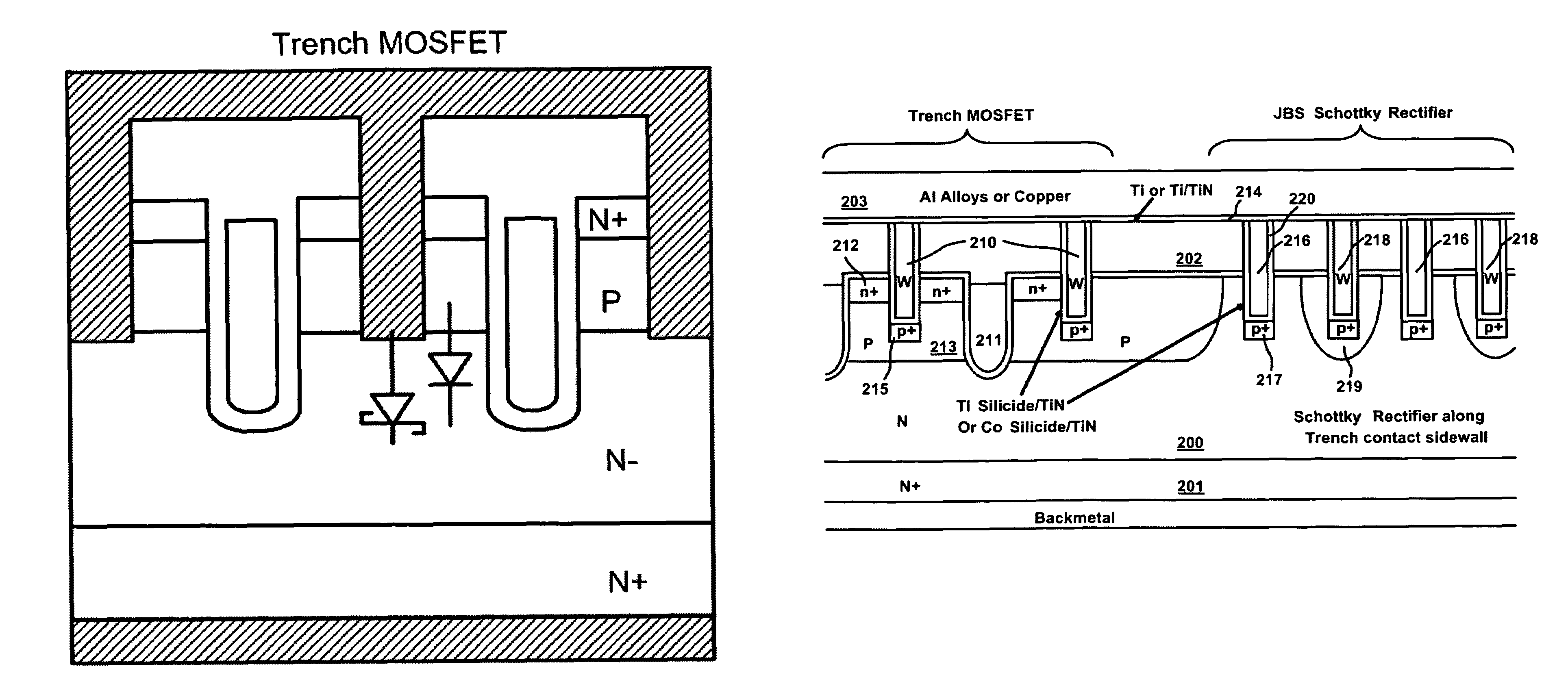
[0031]Please refer to FIG. 6 for a preferred embodiment of this invention where the MOSFET power device with junction barrier Schottky rectifier in one cell are formed in a N epitaxial layer 200 above the a heavily N+ doped substrate 201 coated with back metal on rear side as drain. A trenched gate 211 surrounded by a source region 212 encompassed in a body region 213 formed in a P-well. An insulation layer 202 covering the trenched semiconductor power device with a source-body contact trench 210 opened through and extending into the source and body regions and filled with tungsten plugs therein. A layer of Al Alloys or Copper 203 serves as source metal by a layer of Ti, or Ti / TiN 214 deposited along the top surface of the insulation layer 202. The region 215 is more heavily doped to reduce the resistance between said trench contact metal plug 210 and said body region. The junction barrier Schottky contact trench 216 and more heavily doped region 217 at the bottom of each contact is...


PUM


Abstract

A trench MOSFET in parallel with trench junction barrier Schottky rectifier with trench contact structures is formed in single chip. The present invention solves the drawback brought by some prior arts, for example, the large area occupied by planar contact structure and high gate-source capacitance. As the electronic devices become more miniaturized, the trench contact structures of this invention are able to be shrunk to achieve low specific on-resistance of Trench MOSFET, and low Vf and reverse leakage current of the Schottky Rectifier.

Description

BACKGROUND OF THE INVENTION[0001]1. Field of the Invention[0002]This invention relates generally to the cell structure, device configuration and fabrication process of power semiconductor devices. More particularly, this invention relates to an improved cell configuration and processes to manufacture trench MOSFET device with junction barrier Schottky rectifier in the same cell so that integrated cells with spacing savings and lower capacitance and higher performance are achieved.[0003]2. The Prior Arts[0004]Normally for high efficiency DC / DC application, a Schottky rectifier is externally added in parallel with a MOSFET device. FIG. 1 is a circuit diagram that illustrates the implementation of a Schottky diode with a power MOSFET device. Once the parasitic P / N diode is turned on, both the electron and hole carriers are generated thus require longer time to eliminate the carriers by electron-hole combination. In order to achieve higher speed and efficiency, the Schottky diode (SKY) ...

Claims


Application Information

Patent Timeline
IPC IPC(8): H01L29/76
CPCH01L29/872H01L29/66143H01L29/66727H01L29/66734H01L29/7803H01L29/7813H01L29/861H01L29/0619H01L29/0623H01L29/0878H01L29/41766H01L29/42368H01L29/456H01L29/47
Inventor HSIEH, FU-YUAN
Owner FORCE MOS TECH CO LTD
Why Eureka
Try Eureka