Coreless package substrate with conductive structures

a technology of conductive structure and coreless package, which is applied in the direction of electrical apparatus construction details, non-metallic protective coating applications, and association of printed circuit non-printed electric components, etc., can solve the problems of serious compromise in the manufacture of multi-layer substrates, the thickness of the final multi-layer substrate cannot be reduced, and the use of higher frequency and operation at higher speed is restricted. , to achieve the effect of reducing the thickness of the substrate, raising the wiring density

Inactive Publication Date: 2009-12-01
PHOENIX PRECISION TECH CORP
View PDF4 Cites 24 Cited by
  • Summary
  • Abstract
  • Description
  • Claims
  • Application Information

AI Technical Summary

Benefits of technology

[0012]In light of the shortcomings of the prior arts described above, the primary objective of the present invention is to provide a method of manufacturing a package substrate and to provide a conductive structure of the substrate, so as to raise the wiring density and reduce the thickness of substrate, and thereby meet the developmental trend toward miniaturization.
[0013]Another objective of the present invention is to simplify manufacture steps, raise yield, shorten manufacture time, and reduce manufacture cost.
[0022]Thereby, the coreless package substrate prepared by the present invention has higher circuit layout density, fewer manufacturing steps, reduced general thickness of the products, and a small size.
[0024]In addition, the method of the present invention can further comprise a step (I) after forming solder bumps and solder layer in step (H): attaching at least a metal supporting frame on the surface of the first solder mask, so as to increase general rigidity of the coreless package substrate.
[0025]Besides, the method of the present invention can further comprise a step (G1) before forming the solder bumps in the fourth openings and forming the solder layers in the fifth openings: forming a filling metal layer as a post in at least one of the fourth openings in the first solder mask and the fifth openings in the second solder mask, to thereby reduce the quantity of solder material needed for the solder layers as well as the solder bumps.
[0030]Moreover, the above structure can comprise a metal layer formed in each of the openings of the solder mask as a post before forming the solder layer, to thereby reduce the quantity of solder material needed for the solder layer.

Problems solved by technology

Though high-number leads are achieved in this way, usage on higher frequency and operations at higher speed are restricted due to limited performance of the package structure attributed to lacks of both shorter paths of leads and higher wiring density.
As a result, the thickness of the final multi-layer substrate cannot be reduced, which is unfavorable to the developmental trend of a miniaturized semiconductor package structure.
If the thickness of the core substrate is reduced to as thin as 60 μm or less, the manufacture of the multi-layer substrate will be seriously compromised, and the yield from the manufacture of substrates will decrease significantly.
In addition, there are extra steps in the manufacture of the core substrate, such as the hole-plugging and the scrubbing, which increase the manufacture cost.
In comparison, the process of plating through holes makes it more difficult to form a structure with finer circuits.
Moreover, in the process of the multi-layer substrate described above, it is necessary to fabricate a core substrate prior to forming dielectric layers and circuit layers, which consequently complicates the manufacture steps, prolongs the process, and increases the manufacture cost.
As a result, the industry urgently needs a solution to avoid the drawbacks of the previous technique, such as the increased thickness of a substrate, low wiring density, low yield, complicated manufacture steps, a lengthy process, and a high manufacture cost.

Method used


Image

  • Coreless package substrate with conductive structures
  • Coreless package substrate with conductive structures
  • Coreless package substrate with conductive structures

Examples


Embodiment Construction

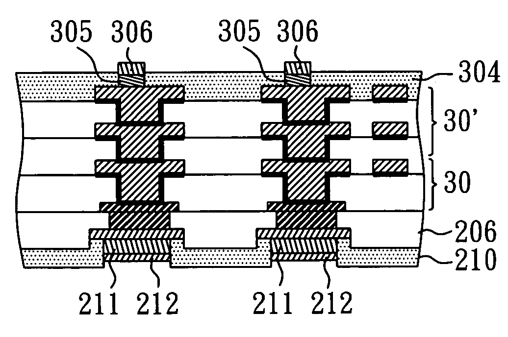
[0034]FIGS. 2A to 2Q are schematic cross-section illustrations of a coreless package substrate of a preferred embodiment of the present invention. First, as shown in FIG. 2A, a metal carrier board 201 is provided. Then, as shown in FIG. 2B, a first resistive layer 202 is formed on the carrier board 201. As shown in FIG. 2C, a plurality of first openings 202a are formed in the first resistive layer to expose parts of the carrier board 201 underneath. Subsequently, as shown in FIGS. 2D and 2E, an etching-stop layer 204 and a first metal layer 205 are in turn formed in the first openings 202a. In this example, the first resistive layer 202 is a dry-film photoresistive layer.

[0035]Referring to FIG. 2F, the first resistive layer 202 is removed. As shown in FIG. 2G, a dielectric layer 206 made of ABF (Ajinomoto Build-up Film) is formed on the surfaces of the carrier board 201 and the first metal layer 205, wherein a plurality of openings 206a is formed by laser ablation in the dielectric ...


PUM

PropertyMeasurementUnit
thicknessaaaaaaaaaa
diameteraaaaaaaaaa
diameteraaaaaaaaaa

Abstract

A method of manufacturing a coreless package substrate together with a conductive structure of the substrate is disclosed. The method can produce a coreless package substrate which comprises: at least a built-up structure having a first solder mask and a second solder mask, wherein a plurality of openings are formed in the first and second solder mask to expose the conductive pads of the built-up structure; and a plurality of solder bumps as well as solder layers formed on the conductive pads. Therefore, the invention can produce the coreless package substrate with high density of circuit layout, less manufacturing steps, and small size.

Description

BACKGROUND OF THE INVENTION[0001]1. Field of the Invention[0002]The present invention relates to a method of manufacturing a core-less package substrate, and more particularly, to a method of manufacturing a coreless substrate that is applicable to non-through hole structures, together with a conductive structure of the substrate, so as to increase integration, and simplify manufacture process.[0003]2. Description of Prior Arts[0004]With rigorous development of the electronic industry, the directions of the research in electronic products are turning to high integration and miniaturization to meet the needs for multi-function, high speed, and high frequency. Accordingly, the circuit board for connecting a plurality of active and passive components to circuits is evolving from single layer to multi-layers in order to expand spaces of circuit layout to thereby meet the requirements of high wiring density for integrated circuits.[0005]The conventional processes of electronic devices be...

Claims


Application Information

Patent Timeline
Patent Type & Authority Patents(United States)
IPC IPC(8): H01L23/48H05K1/03H05K7/00
CPCH01L21/4857H01L23/49822H05K3/4682H05K1/113H05K3/205H05K3/243H05K3/28H01L2924/0002H05K2201/09563H05K2201/096H05K2203/0361H05K2203/0384H01L2924/00
Inventor CHEN, BO-WEIWANG, HSIEN-SHOUHSU, SHIH-PING
Owner PHOENIX PRECISION TECH CORP
Why Eureka
Try Eureka