Automatic clock synchronization and distribution circuit for counter clock flow pipelined systems

a distribution circuit and clock flow technology, applied in the direction of generating/distributing signals, pulse techniques, instruments, etc., can solve the problems of occupying a significant amount of space, requiring a large number of high-power clock distribution buffers, and requiring a large amount of hea

Inactive Publication Date: 2009-12-01
NAVY UNITED STATES OF AMERICA THE REPRESENTED BY THE SEC
View PDF6 Cites 23 Cited by
  • Summary
  • Abstract
  • Description
  • Claims
  • Application Information

AI Technical Summary

Problems solved by technology

There are two major problems with this method of splitting and distributing the clock signal.
First, it requires a large number of high-power clock distribution buffers.
The large number of high-power buffers consumes a large amount of electrical power, generates a large amount of heat, takes up a significant amount of space, and increases system complexity and component count, which decreases reliability and increases cost.
Second, the use of a clock distribution tree does not guarantee that all modules will receive an in-phase clock signal.
Furthermore, the more modules in the system, the more levels will be required in the clock distribution tree, and the greater will be the skew.
It is important to note that all of these major disadvantages exist whenever a pipelined architecture utilizes a synchronous clock, regardless of whether the architecture is applied at the system level, the subcomponent level, or at any level in between.
Unfortunately, the vast majority of pipelined electronic systems require a clock for synchronization.
There are four major advantages and one major disadvantage to using the counter clock flow method for distributing the clock signal in a pipelined circuit or system.
Furthermore, each individual buffer circuit is physically smaller, thus providing a size advantage as well as a power consumption advantage, which can be critically important issues if all components are implemented on a single VLSI integrated circuit.
However, in practice, this is impossible because all clock buffers have slightly different delays, even when implemented on the same integrated circuit.
Furthermore, the different wires that carry the different clock signals between the different buffers, or between the buffers and the processing modules, will also have slightly different delays.
This is not a problem if the total delay from the clock input to module A is greater than the total delay from the clock input to module B. However, in the tree arrangement, this cannot be guaranteed.
If they are not synchronized, a wide variety of difficult problems can occur, such as switching hazards, races, and metastability problems.
However, this can be very difficult to accomplish using a tree structured clock distribution scheme.
This can cause a large number of problems such as noise margin degradation, cross talk, and timing and skew problems.
There is one significant disadvantage to the clock distribution method.
These buffers cause delay, as do the wires that interconnect the clock buffers.
Furthermore, the exact amount of delay is very difficult to predict in advance.
When the data input to the first data processing module is out of phase with the clock signal applied to that stage, a wide variety of difficult problems can occur, including switching hazards, races, and metastability problems.
However, this causes skew between the output data from the last module in the pipeline and the input clock signal.
This disadvantage is so significant that it has prevented the widespread adoption of the counter clock flow pipelined architecture.

Method used


Image

  • Automatic clock synchronization and distribution circuit for counter clock flow pipelined systems
  • Automatic clock synchronization and distribution circuit for counter clock flow pipelined systems
  • Automatic clock synchronization and distribution circuit for counter clock flow pipelined systems

Examples


Embodiment Construction

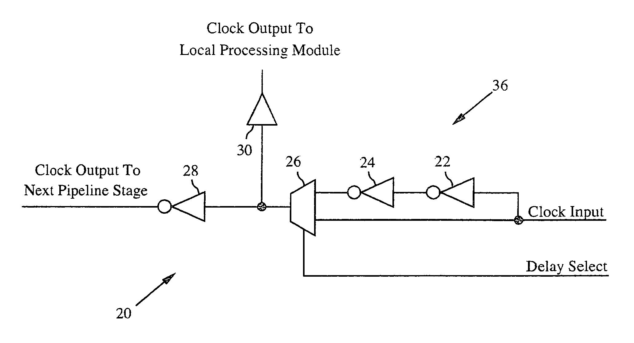
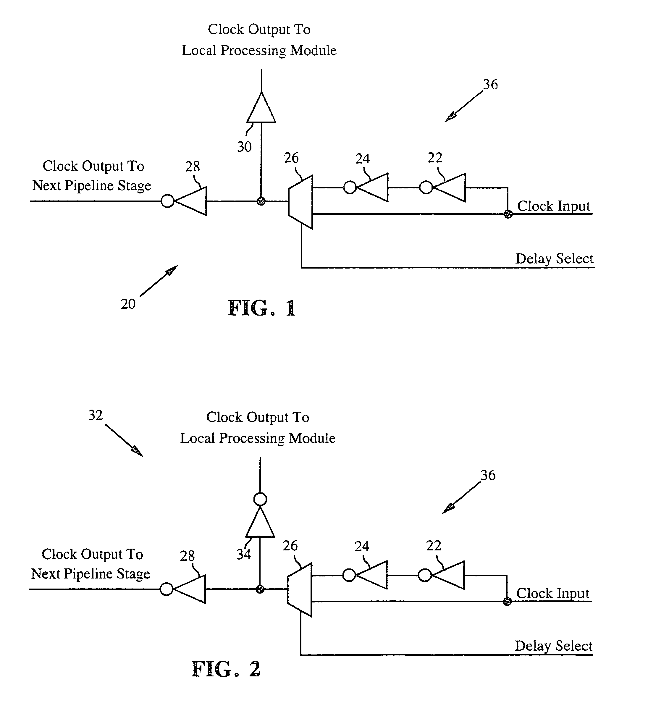
[0026]FIG. 1 illustrates a non-inverting clock synchronization buffer circuit 20 according to the present invention. A pair of inverters 22 and 24 is connected in series with the output of the inverter 24 being connected to a first input of a multiplexer 26. A Clock Input signal is input to the inverter 22 and to a second input of the multiplexer 26. A Delay Select signal is input to a third input of the multiplexer 26. The signal output from the multiplexer 26 is input to an inverting amplifier 28, which provides a Clock Output signal to a next pipeline stage (not shown in FIG. 1). The signal output from the multiplexer 28 is also input to a non-inverting amplifier 30, which provides a Clock Output signal to a local processing module (not shown in FIG. 1).

[0027]FIG. 2 illustrates an inverting second clock synchronization buffer circuit 32 that is similar to the clock buffer circuit 20 with the only difference being that in the inverting clock synchronization buffer circuit has an i...


PUM


Abstract

A clock synchronization buffer for a counter clock flow pipelined circuit including a cascade of processing modules that receive data from a previous module and provide output results to a following module. The clock synchronization buffer receives a clock input signal and provides clock signals to a local processing module and to the next pipeline stage. The clock synchronization buffer includes a selectable delay stage that receives a clock input signal and a delay select signal and outputs a clock signal having a selected delay. An amplifier connected to the selectable delay stage provides the delayed clock signal to a local processing module that corresponds to the clock synchronization buffer circuit. An inverting amplifier connected to the selectable delay stage provides the delayed clock signal to the next pipeline stage. A clock synchronization controller synchronizes the phases of reference clock input and synchronized clock input signals.

Description

BACKGROUND OF THE INVENTION[0001]1. Field of the Invention[0002]2. Description of the Prior Art[0003]Many electronic systems, especially but not limited to digital electronic systems, are composed of a cascade of modules where each module receives input data from one or more previous modules in the cascade, processes the received data, and then sends output results to one or more following modules in the cascade. This architecture is sometimes referred to as a pipelined system or a pipelined circuit and can be applied at the system level, the subsystem level, the component level, or even at the subcomponent level, such as inside an integrated circuit. If all modules are required to work synchronously with all other modules, a clock signal must be distributed to all modules in the system. The normal method used to distribute the clock is to systematically split the signal using buffers to form a clock distribution tree. This ensures that each module receives a clock signal that is in...

Claims


Application Information

Patent Timeline
Patent Type & Authority Patents(United States)
IPC IPC(8): H04J3/06
CPCG06F1/04G06F9/3869H03K5/131H03L7/085H03L7/0805H03L7/0812H03K5/135H03K2005/00058H03L7/0814
Inventor FOUTS, DOUGLAS JAILUKE, BRIAN LEE
Owner NAVY UNITED STATES OF AMERICA THE REPRESENTED BY THE SEC
Why Eureka
Try Eureka