Light-emitting device and electric appliance

a technology of light-emitting devices and electric appliances, which is applied in the direction of semiconductor devices, electrical appliances, instruments, etc., can solve the problems of increasing the manufacturing cost of the device, difficult to ensure a satisfactory yield, and one row of pixels not working, so as to simplify the process of manufacturing the el light-emitting device and improve the yield of the manufacturing process. , the effect of simplifying the need for the process steps of forming p-channel tfts

Inactive Publication Date: 2009-12-15
SEMICON ENERGY LAB CO LTD
View PDF90 Cites 36 Cited by
  • Summary
  • Abstract
  • Description
  • Claims
  • Application Information

AI Technical Summary

Benefits of technology

[0047]According to the embodiment mode of the present invention, all the TFTs are formed as n-channel TFTs so that the need for the process steps for forming p-channel TFTs is simplified, thereby simplifying the process of manufacturing the EL light-emitting device. The yield of the manufacturing process is thereby improved and the manufacturing cost of the EL light-emitting device can be reduced.

Problems solved by technology

Active-matrix EL light-emitting devices, however, have a drawback in that a complicated TFT fabrication process increases the manufacturing cost of the device.
Moreover, since a plurality of TFTs are formed simultaneously, the manufacturing process may be so complicated that it is difficult to ensure a satisfactory yield.
In particular, an operation failure in the driver circuits may result in a line defect such that one row of pixels do not operate.
However, if the drive voltage is increased, there is apprehension that the degradation the organic EL element film is promoted.

Method used


Image

  • Light-emitting device and electric appliance
  • Light-emitting device and electric appliance
  • Light-emitting device and electric appliance

Examples


embodiment 1

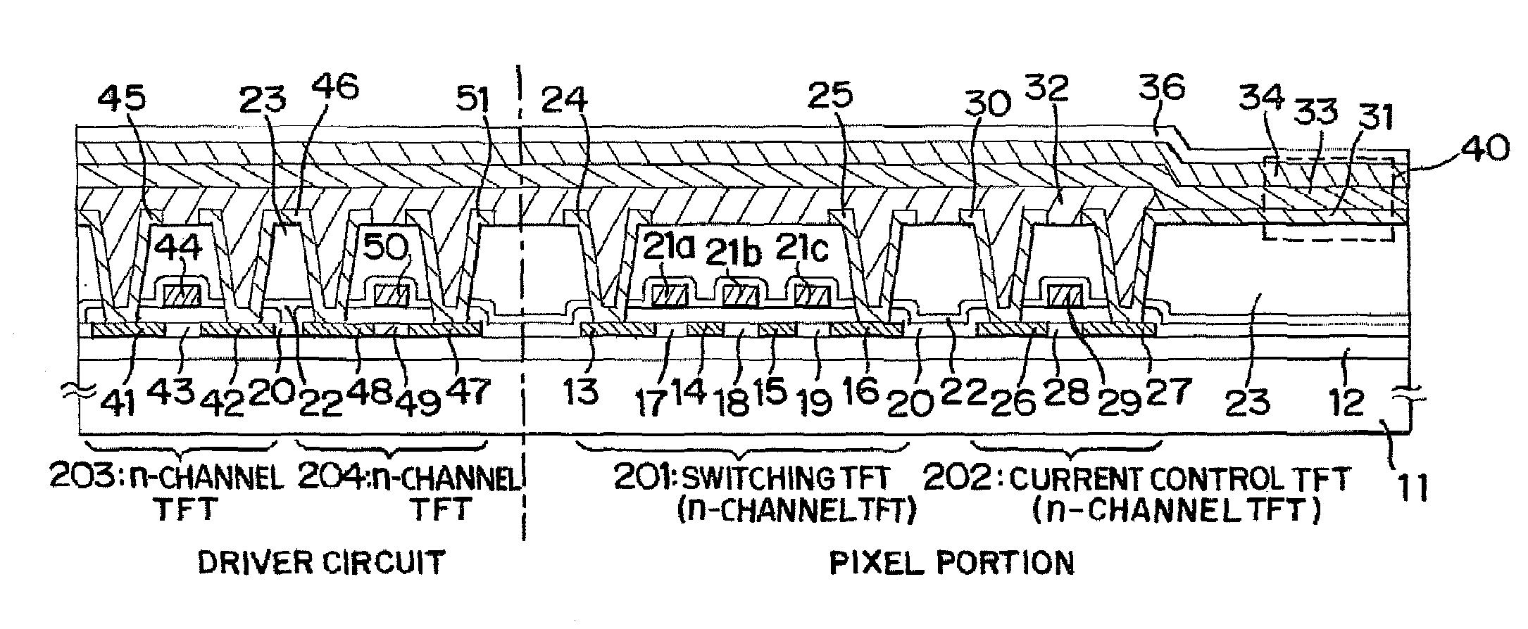
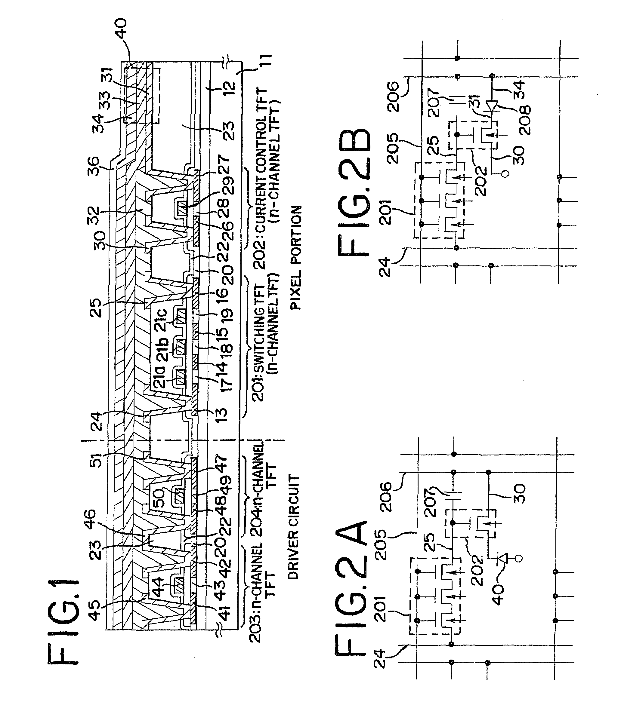
[0069]In this embodiment, the method of manufacturing the pixel portion and the driver circuit to be formed in the periphery thereof on the same insulating body is explained. However, to simplify the explanation, the NMOS circuit combining the n-channel TFT in regards to the driver circuit is shown.

[0070]As shown in FIG. 5A, first an insulator 501 made of plastic is prepared. In this embodiment, as an insulator 501 made of plastic, an insulator coated with protecting films (carbon film, specifically a diamond-like carbon film) 501b and 501c on both sides (the front surface and the back surface) of a plastic substrate 501a is prepared.

[0071]Next, a base film 502 is formed covering the insulator 501 with a thickness of 300 nm. In this embodiment, a silicon nitride oxide film is laminated by a sputtering method to form the base film 502. At this time, a nitrogen concentration of layers contacting the insulator 501 is made to be 10 to 25 wt %, and nitrogen may be included higher than ot...

embodiment 2

[0130]Embodiment 2 will be described with reference to FIGS. 10A and 10B with respect to an example of a structure for enclosing an EL element, which is different from that of the EL light-emitting device in Embodiment 1. Portions identical or corresponding to those shown in FIGS. 9A and 9B are indicated by the same reference characters. FIG. 10B is a cross-sectional view taken along the line A-A′ of FIG. 10A.

[0131]In this embodiment, a plastic film 1001a having its both surfaces coated (covered) with carbon films (specifically, diamond-like carbon films) 1001b and 1001c formed as protective films is used as an insulating member 1001 on which TFTs and an EL element are formed. To form carbon films 1001b and 1001c on the both surfaces of the plastic film 1001a, a roll to roll method may be used.

[0132]By using a sealing material 907, a cover member 1002 is attached to the substrate with the EL element fabricated in accordance with Embodiment 1. A plastic film similar to the plastic fi...

embodiment 3

[0133]Embodiment 3 will be described with respect to a case where in the light-emitting device in accordance with Embodiment 1, the n-channel TFT 601 is formed as a depletion-type TFT and each of the n-channel TFT 602, the switching TFT 603 and the current control TFT 604 is formed as an enhancement-type TFT.

[0134]The portions of the light-emitting device in the state shown in FIG. 5A are completed by the same process as that in Embodiment 1. A silicon oxide film 1101 having a thickness of 100 to 150 nm is then formed by sputtering, and a resist mask 1102 is formed on the region where the n-channel TFT 601 is formed. (FIG. 11A)

[0135]Next, an element belonging to the group 13 in the periodic table (boron in this embodiment) is added to the crystalline semiconductor film 503 by using the resist mask 1102. A region 1103 where boron has been added at a concentration of 1×10¹⁵ to 5×10¹⁷ atoms / cm3 (typically, 1×10¹⁶ to 1×10¹⁷ atoms / cm3) and a region 1104 where no boron has been added are ...


PUM


Abstract

An inexpensive light emitting device capable of displaying a bright image and an electric appliance using the light emitting device. In the light emitting device having a pixel portion and a driver circuit formed on one insulating member, all of semiconductor elements for the pixel portion and the driver circuit are formed by n-channel semiconductor elements, thereby enabling the manufacturing process to be simplified. Each of light-emitting elements provided in the pixel portion emits light in such a direction that most of the light travels away from the insulating member, so that substantially the whole of the pixel-forming segment electrode (corresponding to a cathode of an EL element) is formed as an effective light-emitting area. Therefore, a low-priced light-emitting device capable of displaying a bright image can be obtained.

Description

BACKGROUND OF THE INVENTION [0001]1. Field of the Invention[0002]The present invention relates to a light-emitting device which includes an insulating member, a pixel portion and driver circuits for supplying signals to the pixel portion, and in which the pixel portion and the driver circuits are formed on the same insulating member. Specifically, the present invention includes techniques effective in improving a device having an element constituted of a pair of electrodes and a thin film of a light-emitting material interposed between the pair of electrodes (which element will be hereinafter referred to as “light-emitting element”) (which device will be hereinafter referred to as “light-emitting device”). The light-emitting device of the present invention covers an organic electro-luminescent (EL) display and an organic light-emitting diode (OLED).[0003]In particular, the present invention includes techniques effective in improving a device having an element constituted of an anode...

Claims


Application Information

Patent Timeline
Patent Type & Authority Patents(United States)
IPC IPC(8): G09G3/32H01L27/32
CPCG09G3/3266G09G3/3275H01L27/156G09G3/32G09G2300/0408G09G2300/0842G09G2300/0857H01L27/3244G09G2300/0809H10K59/12
Inventor YAMAZAKI, SHUNPEIKOYAMA, JUNTAKAYAMA, TORU
Owner SEMICON ENERGY LAB CO LTD
Why Eureka
Try Eureka