Transistor, memory cell array and method of manufacturing a transistor

a memory cell array and transistor technology, applied in the field of transistors, can solve the problems of difficulty in providing a surface contact to a stack capacitor, difficulty in integrating a vertical transistor with a stack capacitor, and insufficient isolation properties of access transistors in non-addressed states, so as to achieve the effect of reducing contact resistance, maintaining source/drain region width, and reducing the influence of passing wordlines on adjacent active areas

Inactive Publication Date: 2009-12-22
POLARIS INNOVATIONS LTD
View PDF20 Cites 23 Cited by
  • Summary
  • Abstract
  • Description
  • Claims
  • Application Information

AI Technical Summary

Benefits of technology

[0021]According to a preferred embodiment the distance between said top side and said substrate surface, measured in a direction perpendicular to said substrate surface, is 10 to 200 nm. If the distance between the top side and the substrate surface is smaller than 10 nm the advantageous effects of the present invention will be too weak. On the other hand, if the distance between the top side and the substrate surface is larger than 200 nm, the channel length and, as a consequence, the channel resistance will remarkably be increased.
[0022]Moreover, the present invention provides a memory cell array including a plurality of memory cells, a plurality of bitlines which are arranged in a first direction and a plurality of wordlines which are arranged in a second direction intersecting said first direction, a memory cell including a storage capacitor, a transistor, which is at least partially formed in a semiconductor substrate, said transistor including a first source / drain region, a second source / drain region, a channel region connecting said first and second doped regions, said channel region being disposed in said semiconductor substrate and a gate electrode disposed along said channel region and being electrically insulated from said channel region, said gate electrode controlling an electrical current flowing between said first and second source / drain regions, wherein said channel region includes a fin-region in which the channel has the shape of a fin, said fin including a top side and two lateral sides in a cross section perpendicular to a line connecting said first and second source / drain regions, wherein said top side is disposed beneath a surface of said semiconductor substrate and said gate electrode is disposed along said top side and said two lateral sides, wherein each of said wordlines is electrically connected with a plurality of gate electrodes, and wherein said second source / drain region of each of said transistors is connected with one of said bitlines via a bitline contact.
[0023]In addition, the present invention provides a method of manufacturing a transistor in a semiconductor substrate, including the steps of providing said semiconductor substrate, defining two isolation trenches a surface of said semiconductor substrate, for laterally confining an active area in which the transistor is to be formed, filling said isolation trenches with an insulating material, providing a gate electrode which is insulated from said active area by a gate insulating material, providing a first and a second source / drain regions, wherein a conductive channel is formed between said first and second source / drain regions, a first direction being defined by a line connecting said first and second source / drain regions, wherein said step of providing a gate electrode includes the steps of defining a groove in said active area, said groove extending from said surface of said semiconductor substrate in a direction perpendicular to said surface to a first depth, thereafter, defining a pocket in each said isolation trenches at a position adjacent to said groove so that said two pockets will be connected with said groove and said groove is disposed between said two pockets, said two pockets extending to a second depth larger than said first depth, providing a gate insulating material at an interface between said active area and said groove and at an interface between said active area and said pockets, depositing a gate electrode material so as to fill said groove and said two pockets, partially removing said gate electrode material so that said gate electrode material is removed from the portions outside said groove and said two pockets.
[0024]According to the present invention, since the step of providing a gate electrode includes the step of forming a groove in the active area thereby defining the recessed channel portion, it is possible to align the recessed channel with the gate electrode.
[0025]According to a preferred embodiment, the method further includes the step of thinning the active area at a portion between said first and second depths in a direction parallel to said substrate surface and perpendicular to said first direction.
[0026]Thereby, it is possible to locally thin the active area at the channel region which will later be enclosed by the gate electrode, while maintaining the area of the active region outside the gate electrode region. In particular, the width of the source / drain regions is maintained. As a consequence, the junction contact area will not be thinned whereby a contact resistance is reduced.

Problems solved by technology

There is a lower boundary of the channel length of the access transistor, below which the isolation properties of the access transistor in an non-addressed state are not sufficient.
One of the problems involved with such a vertical transistor cell is the difficulty in providing a surface contact to a stacked capacitor.
Accordingly, such a vertical transistor is difficult to integrate with a stack capacitor.

Method used


Image

  • Transistor, memory cell array and method of manufacturing a transistor
  • Transistor, memory cell array and method of manufacturing a transistor
  • Transistor, memory cell array and method of manufacturing a transistor

Examples


first embodiment

[0054]FIGS. 2A to 2W illustrate the present invention, in which a memory cell array including a transistor of the present invention and a trench capacitor are implemented.

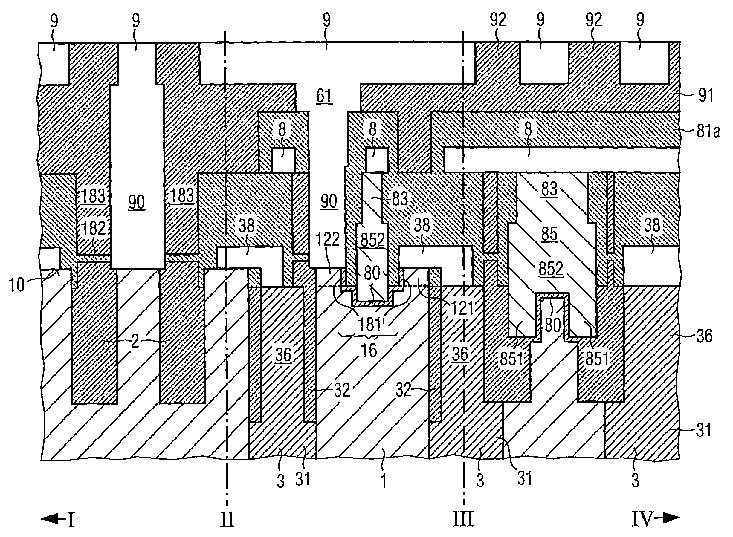
[0055]FIG. 2A illustrates a plan view on the memory cell array, including a plurality of memory cells 100, each memory cell including a trench capacitor 3 and a transistor 16. A plurality of word lines 8 is arranged in a first direction, and a plurality of bit lines is arranged perpendicularly to the word lines 8. Also illustrated in FIG. 2A are the sites I, II, III and IV, which illustrate the directions along which the cross-sectional views illustrated in FIG. 2B, for example, are taken.

[0056]More specifically, the cross-sectional view from I to II illustrates a cross-section perpendicular to a bit line between two adjacent word lines 8, whereas the cross-sectional view from II to III illustrates a cross-section perpendicular to the word lines along a bit line 9, and the cross-sectional view from III to IV illust...

second embodiment

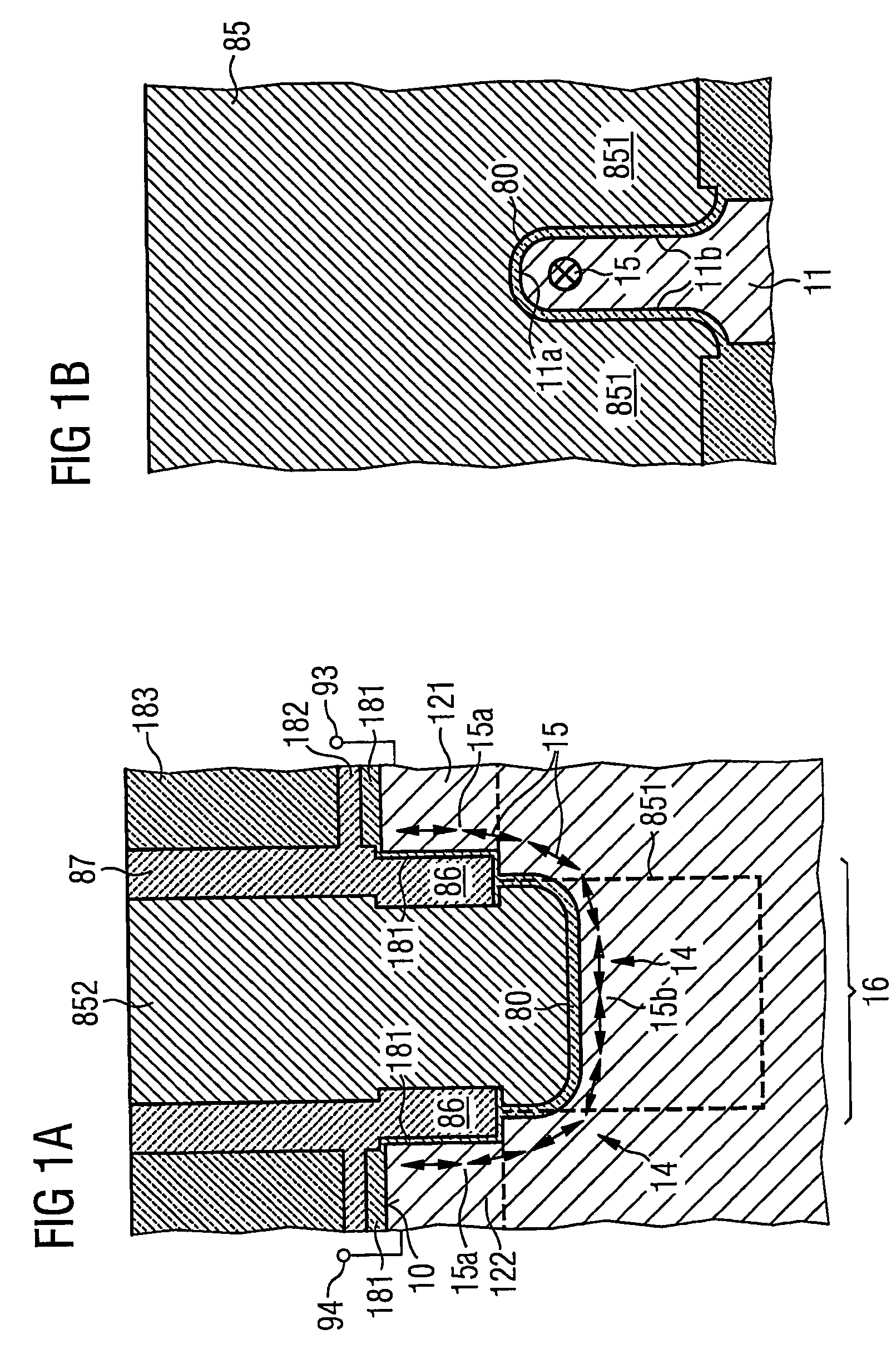
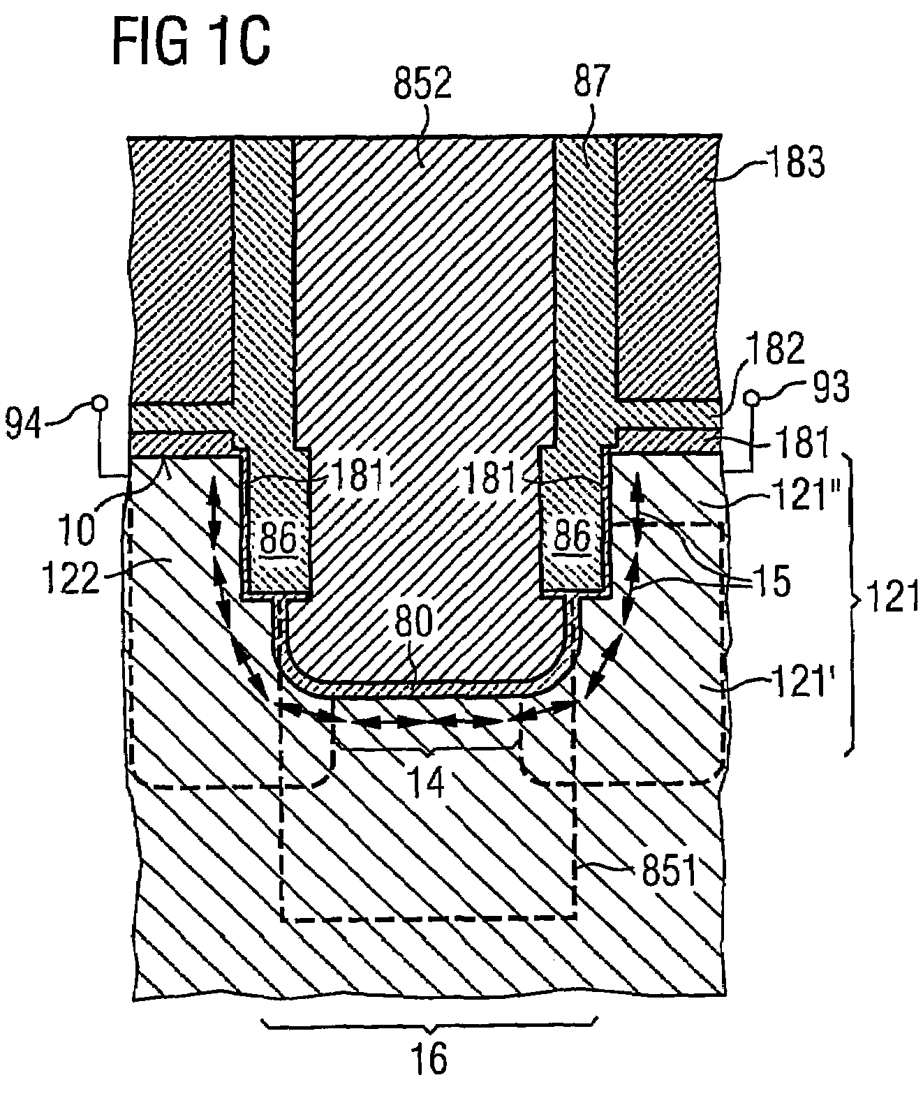
[0093]FIGS. 3A to 3L illustrate the present invention, in which a memory cell includes a stacked capacitor and the transistor which is described above with reference to FIGS. 1A and 1B.

[0094]FIG. 3A illustrates a layout of the active areas 12 of the memory cell array. As illustrated in FIG. 3A two active areas 12 in which the transistor is to be formed are disposed adjacent to each other, and they share a common bit line contact 90 which is indicated by broken lines. The stacked capacitors 4 belonging to each of the memory cells 100 are also indicated by broken lines 4. The segments of the active areas 12 are separated from each other by isolation trenches 23.

[0095]The sectional views illustrated in FIGS. 3B, 3C, 3F, 3G, and 3J are taken between the points V and V.

[0096]For providing the memory cell array according to the second embodiment of the present invention, first, isolation trenches 23 are photolithographically defined and etched in the surface 10 of a semiconductor substrat...

third embodiment

[0118]For implementing the present invention, first, a pad oxide layer (not illustrated) and a silicon nitride layer 17 are deposited on the surface 10 of a semiconductor substrate 1, in particular, a silicon substrate 1. Thereafter, the active areas 12 of the memory cell are photolithograghically defined by known methods and isolation trenches 23 are etched in a common manner so as to expose the active areas 12. The sidewalls of the active areas are oxidized, and the isolation trenches 23 are filled with an insulating material, in particular, a silicon dioxide layer. The resulting surface is planarized. The resulting structure is illustrated in the lower part of FIG. 4A, whereas the upper part of FIG. 4A illustrates a plan view on the array. As can be gathered from the upper part of FIG. 4A, the line connecting VI and VII intersects the active area 12, whereas the line connecting VII and VIII intersects the isolation trenches 23 as well as the active area 12 at the smaller side the...


PUM


Abstract

A transistor, memory cell array and method of manufacturing a transistor are disclosed. In one embodiment, the invention refers to a transistor, which is formed at least partially in a semiconductor substrate, comprising a first and a second source / drain regions, a channel region connecting said first and second source / drain regions, said channel region being disposed in said semiconductor substrate, and a gate electrode disposed along said channel region and being electrically insulated from said channel region, for controlling an electrical current flowing between said first and second source / drain regions, wherein said channel region comprises a fin-region in which the channel has the shape of a ridge, said ridge comprising a top side and two lateral sides in a cross section perpendicular to a line connecting said first and second source / drain regions, wherein said top side is disposed beneath a surface of said semiconductor substrate and said gate electrode is disposed along said top side and said two lateral sides.

Description

CROSS-REFERENCE TO RELATED APPLICATIONS[0001]This Utility Patent Application is a continuation-in-part of U.S. patent application Ser. No. 10 / 939,255, entitled “TRANSISTOR, MEMORY CELL ARRAY AND METHOD OF MANUFACTURING A TRANSISTOR,” and having a filing date of Sep. 10, 2004 now U.S. Pat. No. 7,132,333; and claims the benefit of German Patent Application No. DE 10 2004 031 385.7 filed on Jun. 29, 2004, both of which are incorporated herein by reference.FIELD OF THE INVENTION[0002]The present invention relates to a transistor, a memory cell array including a plurality of memory cells incorporating the transistor, as well as a method of manufacturing a transistor.BACKGROUND[0003]Memory cells of a dynamic random access memory (DRAM) comprise a storage capacitor for storing an electrical charge which represents an information to be stored, and an access transistor for addressing the storage capacitor. The access transistor includes a first and a second source / drain regions, a conductive...

Claims


Application Information

Patent Timeline
Patent Type & Authority Patents(United States)
IPC IPC(8): H01L29/772H01L21/336H01L21/8242H01L27/108H01L27/148H01L29/78H01L29/786
CPCH01L27/10876H01L27/10894H01L29/66621H01L29/7834H01L27/10879H01L27/10808H01L27/10838H01L29/7851H10B12/39H10B12/31H10B12/056H10B12/053H10B12/09
Inventor WEIS, ROLFSCHLOESSER, TILLVON SCHWERIN, ULRIKE GRUENING
Owner POLARIS INNOVATIONS LTD
Why Eureka
Try Eureka