Manufacturing method for ferroelectric memory device

a manufacturing method and memory device technology, applied in the direction of electrical equipment, semiconductor devices, capacitors, etc., can solve the problems of deterioration of ferroelectric capacitor characteristics, reduced ferroelectric film, and need for gap-filling techniques, so as to achieve the effect of reliably preventing deterioration of characteristics

Inactive Publication Date: 2010-01-05
FUJITSU SEMICON LTD
View PDF3 Cites 20 Cited by
  • Summary
  • Abstract
  • Description
  • Claims
  • Application Information

AI Technical Summary

Benefits of technology

[0011]The present invention provides a manufacturing method for a ferroelectric memory device, which enables higher capacitor density described above and prevents the device reliability lowering due to deterioration of the characteristics of the capacitors.
[0013]According to the manufacturing method for a ferroelectric memory device described above, a first hydrogen barrier film and a dielectric film that cover the ferroelectric capacitors are formed. The dielectric film is etched back thereby forming sidewalls on side sections of the ferroelectric capacitors. Then, a second hydrogen barrier film is formed on the sidewalls by a chemical vapor deposition method. Therefore, in a narrow gap portion between adjacent ones of the capacitors, the major part of the gap can be filled by the sidewalls, and a gap remaining between the sidewalls can be filled with a second hydrogen barrier film. More specifically the second hydrogen barrier film can fill the narrow gap between the sidewalls excellently by the aluminum oxide film that has excellent coverage property for example. Furthermore, in a wide gap portion between adjacent ones of the capacitors, the first hydrogen barrier film may be exposed as a result of the etching back process of the dielectric film, and the second hydrogen barrier film is deposited on the first hydrogen barrier film directly, and the interlayer dielectric film is further deposited on it such that the gap is excellently filled. Because aluminum oxide has a high etching resistance, forming contact holes therein is a rather difficult process, and a thick aluminum oxide film gives a disadvantage to the process. However, by the manufacturing method in accordance with the present invention, the major part of the gap between adjacent capacitors can be filled with sidewalls of the dielectric film, such that a small gap remaining between the sidewalls can be desirably filled, even if a rather thin barrier film is used as the second hydrogen barrier film.
[0014]Also, the ferroelectric capacitor is covered by the first and the second hydrogen barrier films, and the ferroelectric capacitor is well guarded from the hydrogen attack. Accordingly, by the manufacturing method in accordance with the aspect of the invention, a ferroelectric memory device can be obtained with a higher capacitor density and preventing the reliability lowering due to deterioration of the characteristics.
[0016]As described above, aluminum oxide film deposited by the CVD method has excellent coverage, such that relatively narrow gaps between capacitors and narrow gaps between sidewalls can be desirably filled.
[0018]By the atomic layer chemical vapor phase deposition method that is a type of chemical vapor deposition methods, the coverage property can be improved, such that, even when a gap between the sidewalls becomes narrower, this narrow gap can be reliably filled.
[0020]As a result, even when moisture or hydrogen remain in the sidewall, the heat treatment can remove it from the sidewall. If moisture or hydrogen remains in the sidewall, it sealed by the second hydrogen barrier film at the next step, and cannot be removed thereafter. Therefore, this moisture or hydrogen would diffuse into the dielectric films of the product, which cause deterioration of the capacitor characteristics and damage the device reliability. However, by removing moisture and hydrogen from the sidewall before forming the second hydrogen barrier film, by the heat treatment, deterioration of the characteristics can be reliably prevented.

Problems solved by technology

In the process for manufacturing such a ferroelectric memory device, if the ferroelectric film, after having been formed, is exposed to a reductive atmosphere such as hydrogen (H2) or water (H2O), the ferroelectric film is reduced, such that the electrical characteristics of the ferroelectric material is changed, causing a deterioration of the ferroelectric capacitor characteristics.
However, when the capacitors are densely placed, a gap-fill technique is required for filling gaps between the capacitors with dielectric films.
If the capacitors are covered by a dielectric layer without completely filling of the gaps between the capacitors, unfilled portions remain as voids, residual gas may stay there, and the gas causes the deterioration of the ferroelectric material with the passage of time, whereby the device reliability is lowered.
When the gap between adjacent capacitor becomes so narrow, it would be difficult to fill the gap with the ordinary film forming method described above.
However, in the process for manufacturing ferroelectric memory devices, gaps between the capacitors need to be filled without deteriorating the characteristics of the ferroelectric capacitors as described above, and this requirement causes greater difficulty compared to the case of filling gaps between metal wirings.
The characteristics of the capacitors are damaged by both the high density plasma and the chemical attach of the hydrogen or water generated during the HDP or SOG film formation.
Because aluminum oxide has a high etching resistance, forming contact holes therein is a rather difficult process, and a thick aluminum oxide film gives a disadvantage to the process.
Therefore, this moisture or hydrogen would diffuse into the dielectric films of the product, which cause deterioration of the capacitor characteristics and damage the device reliability.

Method used


Image

  • Manufacturing method for ferroelectric memory device
  • Manufacturing method for ferroelectric memory device
  • Manufacturing method for ferroelectric memory device

Examples


Embodiment Construction

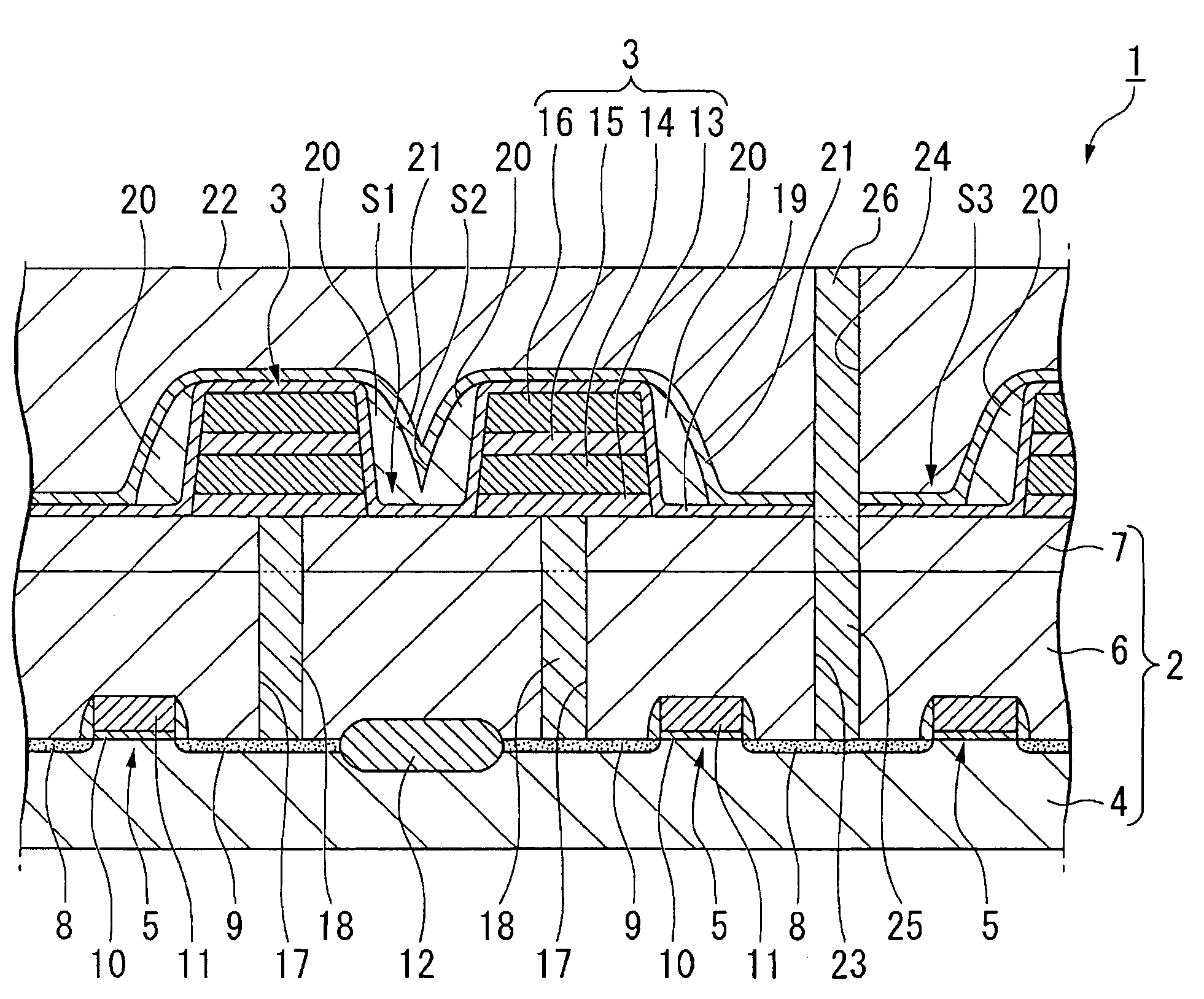
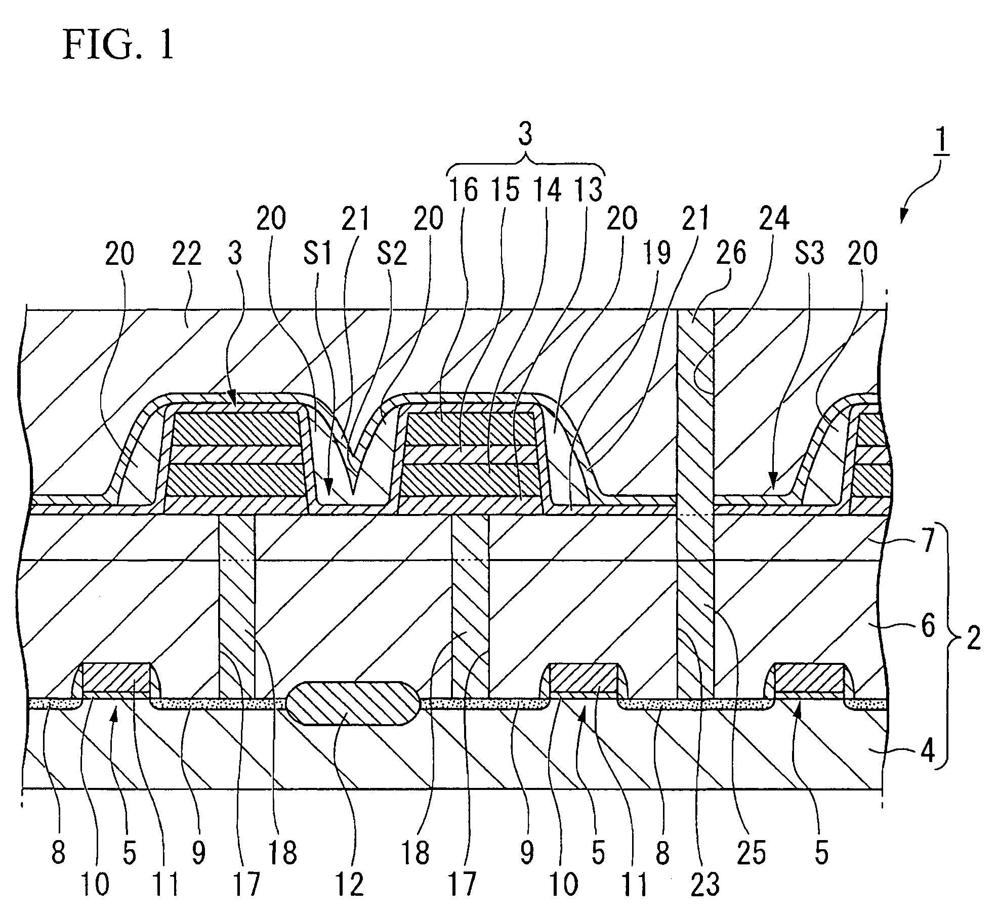
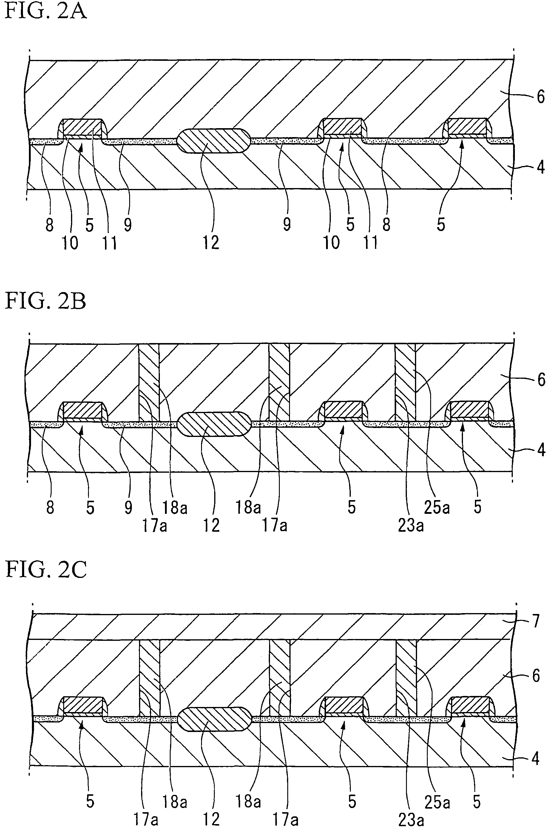
[0026]Preferred embodiments of the invention are described in detail below. Prior to describing a manufacturing method for a ferroelectric memory device in accordance with an embodiment of the invention, an example of the ferroelectric memory device obtained by the method is described. FIG. 1 is a schematic cross-sectional view of a ferroelectric memory device manufactured by the manufacturing method in accordance with an embodiment of the invention. Reference numeral 1 in the figure denotes a ferroelectric memory device. The ferroelectric memory device 1 is a 1T / 1C memory cell structure with a stacked type capacitor, and is equipped on a base substrate 2, and ferroelectric capacitors 3 provided on the base substrate 2. This embodiment is described with reference to a 1T / 1C type memory cell structure, but the invention is not limited to a 1T / 1C type.

[0027]The base substrate 2 is formed on a silicon substrate (a semiconductor substrate) 4. Transistors 5 for operating the ferroelectri...


PUM


Abstract

A manufacturing method for a ferroelectric memory device includes: forming a ferroelectric capacitor on a substrate, the ferroelectric capacitor including a lower electrode, a ferroelectric film, and an upper electrode; forming a first hydrogen barrier film that covers the ferroelectric capacitor by a chemical vapor deposition method; forming a dielectric film on the first hydrogen barrier film; forming a sidewall composed of the dielectric film on a side of the ferroelectric capacitor by etching back the dielectric film; forming a second hydrogen barrier film on the first hydrogen barrier film and the sidewall by a chemical vapor deposition method; and forming an interlayer dielectric film on the second hydrogen barrier film.

Description

CROSS-REFERENCE TO RELATED APPLICATION[0001]This application claims priority from Japanese Patent Application No. 2006-321467, filed on Nov. 29, 2006, the contents of which are incorporated herein by reference.BACKGROUND[0002]1. Technical Field[0003]The present invention relates to a manufacturing method for a ferroelectric memory device having a ferroelectric capacitor.[0004]2. Related Art[0005]A ferroelectric memory device is generally provided with a ferroelectric capacitor having a ferroelectric film composed of metal oxides. In the process for manufacturing such a ferroelectric memory device, if the ferroelectric film, after having been formed, is exposed to a reductive atmosphere such as hydrogen (H2) or water (H2O), the ferroelectric film is reduced, such that the electrical characteristics of the ferroelectric material is changed, causing a deterioration of the ferroelectric capacitor characteristics. In order to prevent this hydrogen damage, usually, a dielectric film havin...

Claims


Application Information

Patent Timeline
Patent Type & Authority Patents(United States)
IPC IPC(8): H01L21/00
CPCH01L27/11502H01L28/65H01L28/57H01L27/11507H10B53/30H10B53/00
Inventor FUKADA, SHINICHISASHIDA, NAOYA
Owner FUJITSU SEMICON LTD
Why Eureka
Try Eureka