Coupling structure for optical fibres and process for making it

a technology of optical fibres and coupling structures, applied in the field of coupling structures for optical fibres and process for making them, can solve the problem that the optical fibre end surface cannot be brought sufficiently close to the optical device to make a low-loss optical connection, and achieve the effect of limiting diffusion or diffraction, and optimising coupling efficiency

Inactive Publication Date: 2010-01-12
PIRELLI & C +1
View PDF17 Cites 12 Cited by
  • Summary
  • Abstract
  • Description
  • Claims
  • Application Information

AI Technical Summary

Benefits of technology

[0011]Applicants have understood that, in order to optimise the coupling efficiency between an optical device and an optical fibre, the space interposed between the fiber end and the active region of the optical device where the light travels without being guided, i.e., through an unguided medium, should be minimised in order to limit diffusion or diffraction.
[0013]It is an object of the present invention to provide a packaging arrangement for a low-cost highly integrated opto-electronic module, which would promote precise and relatively easy fibre-to-optical device insertion and alignment.
[0014]It is to be noted that optical coupling between optical fibres and optical devices that are flip-chip bonded to the coupling structure also benefit from the present invention, as the thickness of the unguided media where the light travels when exiting the optical device or the optical fibre is reduced to the minimum.
[0016]Applicants have further developed a coupling structure comprising a guidance element including a guidance channel, which is integrated to a fibre drive-in element that allows the insertion of the optical fibre. Precise alignment of the optical device to the fibre can be achieved by fabricating the coupling structure with high precision, i.e., of less than 1 μm, and by the accurate placement of the drive-in element to the guidance element so as to align the guidance channel with the fibre, in particular the guidance channel core with the fibre core.

Problems solved by technology

Because of the space required for the wire bond, in case of coupling of the optical device to an optical fibre, the optical fibre end surface cannot be brought sufficiently close to the optical device to make a low-loss optical connection.

Method used


Image

  • Coupling structure for optical fibres and process for making it
  • Coupling structure for optical fibres and process for making it
  • Coupling structure for optical fibres and process for making it

Examples


first embodiment

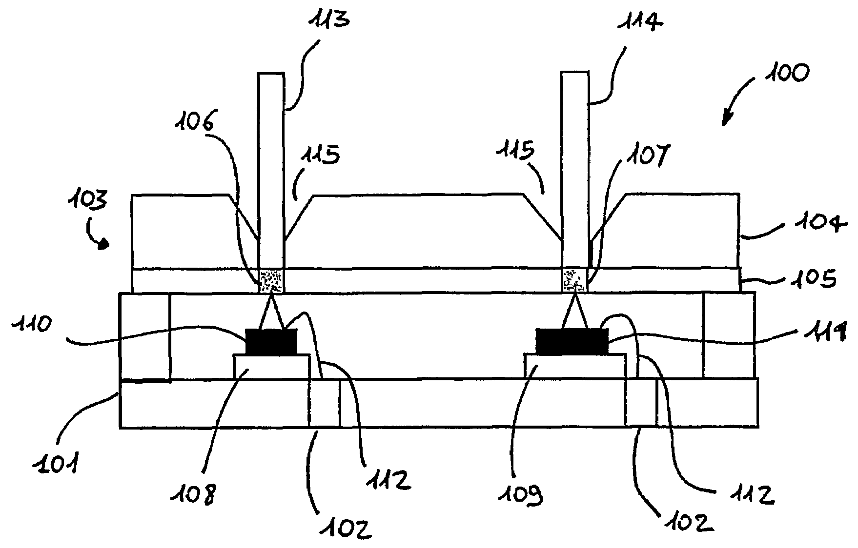
[0058]FIG. 1 illustrates a first preferred embodiment of the coupling structure for coupling an optical fibre to an optical device according to the present invention. Coupling structure, the guidance element 1, comprises a monocrystalline silicon (c-Si) substrate 2 having formed therein a SiO2-based optical through-via 3, or guidance channel, which includes a channel cladding 4 and a channel core 5. In the preferred embodiment, the channel core 5 is substantially made of SiO2 having a refractive index larger than the refractive index of the SiO2 which substantially forms the channel cladding 4. Preferably, the difference in refractive index between the core and the dad channels is of 0.5-0.8%. As it will become clear from the following description, the optical fibre will be coupled to the guidance channel of the guidance element 1 so that the core of the fibre will substantially correspond to the channel core of the guidance channel. Light transmitted from or to the optical fibre wi...

second embodiment

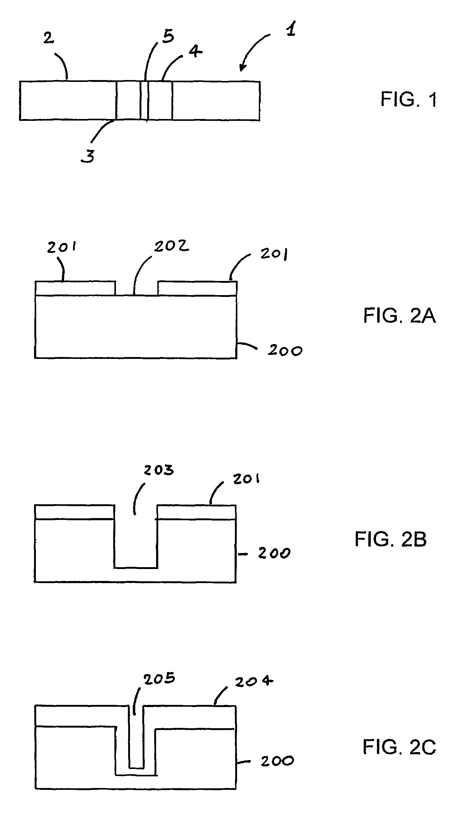
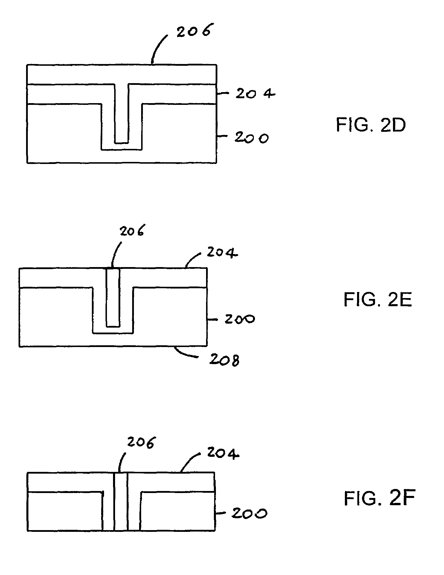
[0062]According to a second embodiment of the present invention, the coupling structure comprises a graded-index guidance channel. FIGS. 3A-3H illustrate the process steps that can be used to obtain the coupling structure with a graded-index channel shown in FIG. 3H. An opening 302 is defined in a silicon oxide mask 301 on a silicon substrate 300 (FIG. 3A). The silicon substrate is for example a 6″ c-Si 675 μm-thick wafer. Preferably, opening 302 is circular and has a diameter about twice the diameter of the desired channel core of the coupling structure. For example, in order to obtain a 9-μm channel core diameter, opening 302 is chosen to be about 18 μm. A deep trench 303 is formed in the silicon substrate 300 through opening 302 by etching, preferably by dry etching (FIG. 3B). Preferably, trench 303 has “sloped” sidewalls. For example, deep reactive ion etching (RIE) is carried out at a temperature of 20° C. for 1 h to form a 200 μm deep trench having a wall taper angle α of 87-8...

third embodiment

[0065]According to a third embodiment of the present invention, the coupling structure comprises a coaxial guidance channel. A silicon oxide layer is grown on a c-Si substrate 400. The silicon oxide 401 is patterned by means of a lithographic mask so as to expose the areas where the trenches are to be formed (FIG. 4A). A non-exposed annular surface 402 is interposed between a first circular opening 411 and an external annular opening 412. The exposed areas are then etched, e.g., by dry etching, to form deep trenches 403 and 404 (FIG. 4B). In a preferred embodiment, trench 404 has a diameter of about 18 μm and external annular trench 403 has a width of about 15 μm. The annular region underneath the non-etched annular surface 402 is preferably 7 μm wide. The oxide 401 is then removed. In a subsequent step, a relatively thick SiO2 layer 405 of refractive index n1 is thermally grown on the substrate surface and within the trenches so as to fully oxidise the annular wall corresponding to...


PUM


Abstract

A coupling structure for coupling optical radiation, i.e., light, between an optical fibre and an optical device, e.g., a laser diode or a photodiode. The coupling structure has an optical through-via which guides the optical radiation to or from the optical fibre. Light exiting the fibre travels through a guidance channel so it remains substantially confined to a narrow optical path that mimics the fibre core. Conversely, light enters the fibre after having traveled through the guidance channel. The guidance channel has a first core region, the “channel core”, having first refractive index surrounded by a second region, the “channel cladding” having a second refractive index smaller than the first refractive index. The coupling structure, including the guidance channel, is preferably made of semiconductor-based material, more preferably of silicon-based material. The guidance channel is preferably silicon oxide. The coupling structure further has a fibre drive-in element, which facilitates insertion and alignment of the optical fibre to the guidance channel.

Description

[0001]The present invention relates to a coupling structure for optical fibres. In particular, the invention relates to a coupling structure suitable for passive alignment of an optical fibre to an optical device, or a plurality of optical fibres to a plurality of optical devices, and its related fabrication method. In addition, the invention concerns an opto-electronic package for connection and alignment of optical fibres.RELATED ART[0002]The demand of high-speed data access and the associated need of more bandwidth for applications such as Internet or Ethernet have recently increased the interest towards the distribution of high-capacity optical fibres directly to customer premises, bringing fibre optics to the so-called “last mile”. Implementation of complete fiber optic networks from a service provider directly to subscriber's premises, such as fibre to the business / home, often generally referred to as fibre-to-the-X (FTTX), is presently still considerably expensive. In order t...

Claims


Application Information

Patent Timeline
Patent Type & Authority Patents(United States)
IPC IPC(8): G02B6/36H01L21/00G02B6/132G02B6/136G02B6/42
CPCG02B6/132G02B6/4206G02B6/136
Inventor MARTINI, FRANCESCOMONTANINI, PIETROOLIVETI, GUIDORAMPULLA, ALBERTOROSSI, GIACOMO
Owner PIRELLI & C
Why Eureka
Try Eureka