

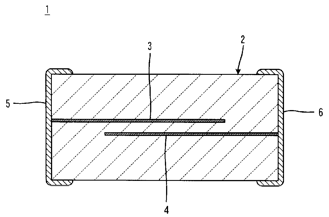
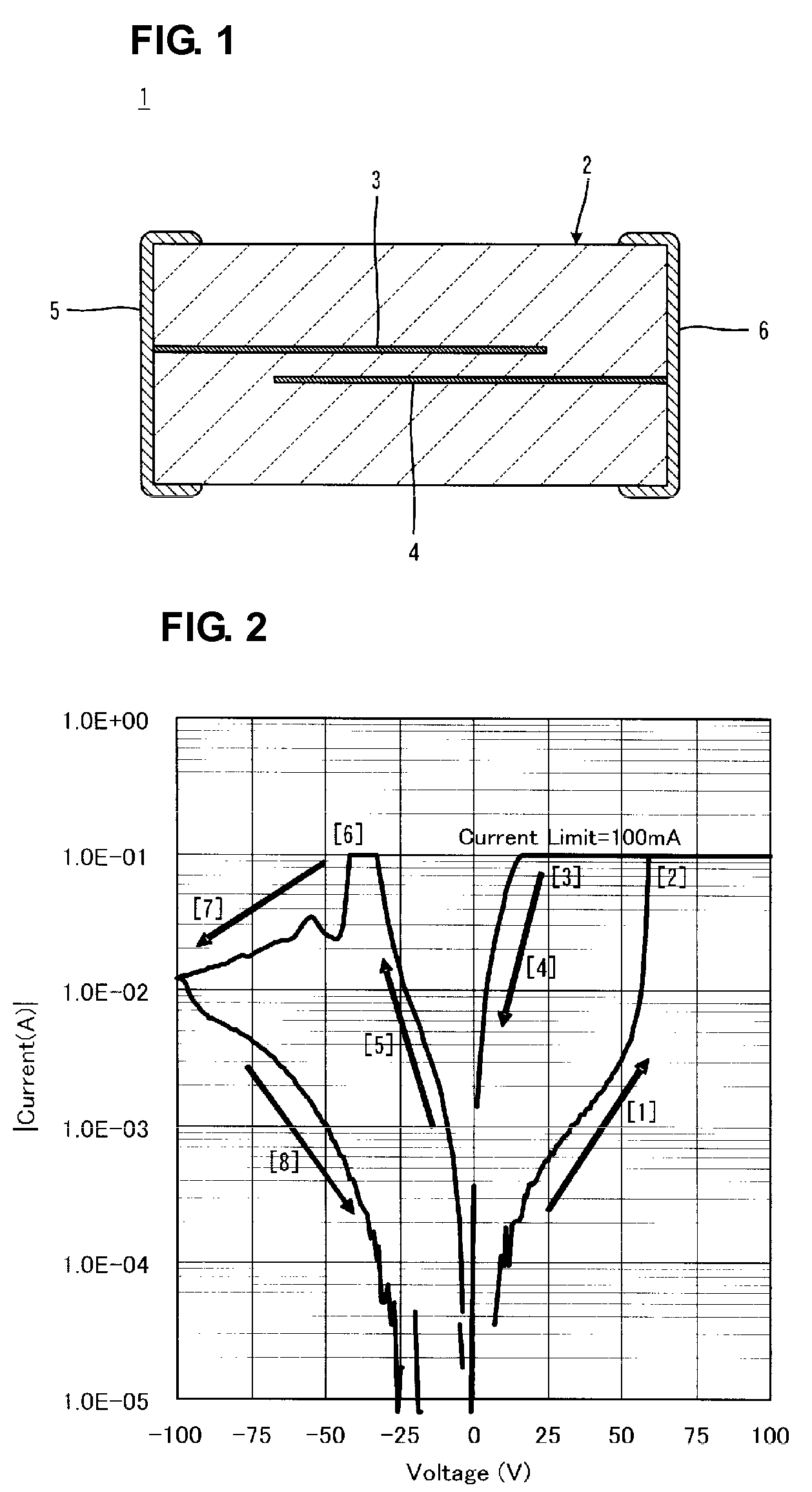
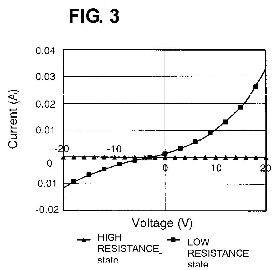
Resistance memory element
a technology of resistor and resistance, applied in the direction of digital storage, instruments, electrical apparatus, etc., can solve the problems of disadvantageously reducing the variation of resistances switched, the element cannot be used as a switching element with a relatively high driving voltage, and the increase in power consumption due to additional resistors, etc., to achieve high switching voltage and high rate
- Summary
- Abstract
- Description
- Claims
- Application Information
AI Technical Summary
Benefits of technology
Problems solved by technology
Method used
Image

Examples
experiment 1
[0054]Powder starting materials were prepared for the strontium titanate-base semiconductor ceramic of the elementary body, including strontium carbonate (SrCO3) and titanium oxide (TiO2); and donors: lanthanum oxide (La2O3), neodymium oxide (Nd2O3), samarium oxide (Sm2O3), gadolinium oxide (Gd2O3), dysprosium oxide (Dy2O3), holmium oxide (Ho2O3), or yttrium oxide (Y2O3) and niobium oxide (Nb2O5) or tantalum oxide (Ta2O5).
[0055]These starting materials were weighed so that the compositions shown in Tables 1 to 5 were produced after firing. Then, a dispersant and water were added to the weighed materials, and the materials were pulverized and mixed together with PSZ balls having a diameter of about 2 mm for about 24 hours in a wet process. After pulverization, the resulting slurry was dried and calcined at about 1200° C. for about 4 hours in the air. A dispersant and pure water were added to the calcined powder, and the powder was pulverized with PSZ balls having a diameter of about ...
experiment 2
[0073]In Experiment 2, the strontium titanate-based semiconductor ceramic of the elementary body having substantially the same composition as Sample 8 in Experiment 1 was prepared, and samples were formed in the same process as in Experiment 1 according to Table 6, and varying the thickness of the green sheets and the firing temperature. Table 6 shows the thickness between the opposing electrodes depending on the thickness of the green sheet and the firing temperature. The reducing conditions depend on the firing temperature and the thickness of the green sheet (between the opposing electrodes). Accordingly, the reducing temperature after firing was appropriately selected from the range of about 600° C. to about 1200° C. for each sample.
[0074]In Experiment 2, the maximum resistance variation and the switching voltage were measured as in Experiment 1, and, in addition, the average particle size of the strontium titanate-based semiconductor ceramic and the average number of grain boun...
experiment 3
[0082]In Experiment 3, strontium titanate-based semiconductor ceramics having the following compositions were prepared for the elementary body:
[0083](1) compositions expressed by (Sr1−xAx)vTiwO3, wherein x (amount of the substituent “A”: La, Nd, Sm, Gd, Dy, Ho, or Y added to the Sr site as a donor) and the ratio v / w of the Sr site to the Ti site were varied as shown in Tables 7 to 13;
[0084](2) compositions expressed by Srv(Ti1−yBy)wO3, wherein y (amount of the substituent “B”: Nb or Ta added to the Ti site as a donor) and the ratio v / w of the Sr site to the Ti site were varied as shown in Tables 14 and 15; and
[0085](3) compositions expressed by (Sr1−xAx)v(Ti1−yNby)wO3, wherein the sum of x (amount of the substituent “A”: La, Sm, Gd, Dy, or Y added to the Sr site as a donor) and y (amount of Nb substitution), x+y, and the ratio v / w of the Sr site to the Ti site were varied as shown in Tables 16 to 20.
[0086]In the compositions of (1), y=0 holds, and x is equal to x+y. In the compositi...
PUM
| Property | Measurement | Unit |
|---|---|---|
| switching voltage | aaaaa | aaaaa |
| rated voltage | aaaaa | aaaaa |
| voltage | aaaaa | aaaaa |
Abstract
Description
Claims
Application Information